
January 1996
INT200
Low-side Driver IC
Low-side Drive and High-side Control
with Simultaneous Conduction Lockout
Product Highlights
5 V CMOS Compatible Control Inputs
∑ Combines logic inputs for low and high-side drives
∑ Schmidt-triggered inputs for noise immunity
Built-in High-voltage Level Shifters
∑ Integrated level shifters simplify high-side interface
∑ Can withstand up to 800 V for direct interface to the
INT201 high-side driver
∑ Pulsed high-voltage level shifters reduce power
consumption
Gate Drive Output for an External MOSFET
∑ Provides 300 mA sink/150 mA source current
∑ Can drive MOSFET gate at up to 15 V
∑ External MOSFET allows flexibility in design for various
motor sizes
Built-in Protection Features
∑ Simultaneous conduction lockout protection
∑ UV lockout
Description
The INT200 Low-side driver IC provides gate drive for an
external low-side MOSFET switch and high-side level shifting.
When used in conjunction with the INT201 high-side driver, the
INT200 provides a simple, cost-effective interface between
low-voltage control logic and high-voltage loads. The INT200
is designed to be used with rectified 110 V or 220 V supplies.
Both high-side and low-side switches can be controlled
independently from ground-referenced 5 V logic inputs on the
low side driver.
Built-in protection logic prevents both switches from turning
on at the same time and shorting the high voltage supply. Pulsed
level shifting saves power and provides enhanced noise
immunity. The circuit is powered from a nominal 15 V supply
to provide adequate gate drive for external N-channel MOSFETs.
Applications include motor drives, electronic ballasts, and
uninterruptible power supplies. The INT200 can also be used
to implement full- bridge and multi-phase configurations.
The INT200 is available in 8-pin plastic DIP and SOIC packages.
Æ
ORDERING INFORMATION
PART
PACKAGE
ISOLATION
NUMBER
OUTLINE
VOLTAGE
INT200PFI1
P08A
600 V
INT200TFI1
T08A
600 V
INT200PFI2
P08A
800 V
INT200TFI2
T08A
800 V
HSD2
HS IN
PI≠284C≠072291
COM
8
5
7
6
N/C
LS IN
LS OUT
1
4
2
3
VDD
HSD1
Figure 2. Pin Configuration.
Figure 1. Typical Application
HV
HS IN
LS IN
INT201
INT200
PI-11762-012396
VDD
3-PHASE
BRUSHLESS
DC MOTOR

INT200
F
1/96
Pin Functional Description
Pin 1:
Active-low logic-level input HS IN
controls the pulse circuit which signals
the INT201 high-side driver.
Pin 2:
Active-high logic level input LS IN
controls the low side driver output.
Pin 3:
LS OUT is the driver output which
controls the low-side MOSFET.
Pin 4:
COM connection; analog reference point
for the circuit.
Pin 5:
Level shift output HSD 2 signals the
high-side driver to turn off. One short,
precise pulse is sent on each positive
transition of
HS IN.
Pin 6:
Level shift output HSD 1 signals the
high-side driver to turn on. Two short,
precise pulses are sent on each negative
transition of
HS IN.
Pin 7:
N/C for creepage distance.
Pin 8:
V
DD
supplies power to the logic, high-
side interface, and low-side driver.
2
Figure 3. Functional Block Diagram of the INT200
HS IN
LS IN
COM
HSD1
HSD2
LS OUT
PI-286F-043093
PULSE
CIRCUIT
LINEAR
REGULATOR
VDD
DELAY
UV
LOCKOUT
F
1/96
INT200
INT200 Functional Description
5 V Regulator
The 5 V linear regulator circuit provides
the supply voltage for the control logic
and high-voltage level shift circuit. This
allows the logic section to be directly
compatible with 5 V CMOS logic
without the need of an external 5 V
supply.
Undervoltage Lockout
The undervoltage lockout circuit disables
the LS OUT pin and both HSD pins
whenever the V
DD
power supply falls
below typically 9.0 V, and maintains
this condition until the V
DD
power supply
rises above typically 9.35 V. This
guarantees that both MOSFETs will
remain off during power-up or fault
conditions.
HSD1/HSD2
The HSD1 and HSD2 outputs are
connected to integrated high-voltage N-
channel MOSFET transistors which
perform the level-shifting function for
communication to the high-side driver.
Controlled current capability allows the
drain voltage to float with the high-side
driver. Two individual channels produce
a true differential communication
channel for accurately controlling the
high-side driver in the presence of fast
moving high-voltage waveforms.
Pulse Circuit
The pulse circuit provides the two high-
voltage level shifters with precise timing
signals. Two pulses are sent over HSD1
to signal the high-side driver to turn on.
One pulse is sent over HSD2 to signal
the high-side driver to turn off. The
combination of differential
communication with the precise timing
provides maximum immunity to noise.
Conduction Latch
An RS latch prevents the low-side driver
and high-side driver from being on at the
same time, regardless of the input signals.
.
Delay Circuit
The delay circuit matches the low-side
propagation delay with the combination
of the pulse circuit, high voltage level
shift, and high-side driver propagation
delays. This ensures that the low-side
driver and high-side driver will never be
on at the same time during switching
transitions in either direction.
Driver
The CMOS drive circuit provides drive
power to the gate of the MOSFET used
on the low side of the half bridge circuit.
The driver consists of a CMOS buffer
capable of driving an external transistor
gate at up to 15 V.
3
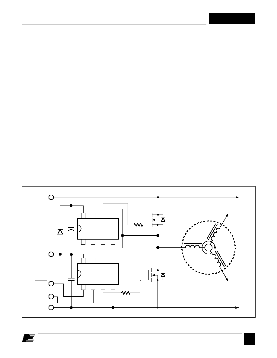
Figure 4. Using the INT200 and INT201 in a 3-phase Configuration.
PI-1461-042695
HV+
VDD
LS IN
HV-
INT201
INT200
PHASE 1
PHASE 2
PHASE 3
3-PHASE
BRUSHLESS
DC MOTOR
D1
C1
C2
R1
R2
Q2
Q1
HS IN
1
2
3
4
8
7
6
5
1
2
3
4
8
7
6
5

INT200
F
1/96
4
General Circuit Operation
One phase of a three-phase brushless
DC motor drive circuit is shown in Figure
4 to illustrate an application of the
INT200/201. The LS IN signal directly
controls MOSFET Q1. The
HS IN signal
causes the INT200 to command the
INT201 to turn MOSFET Q2 on or off as
required. The INT200 will ignore input
signals that would command both Q1
and Q2 to conduct simultaneously,
protecting against shorting the HV+ bus
to HV-.
Local bypassing for the low-side driver
is provided by C1. Bootstrap bias for the
high-side driver is provided by D1 and
C2. Slew rate and effects of parasitic
oscillations in the load waveforms are
controlled by resistors R1 and R2.
The inputs are designed to be compatible
with 5 V CMOS logic levels and should
not be connected to V
DD
. Normal CMOS
power supply sequencing should be
observed. The order of signal application
should be V
DD
, logic signals, and then
HV+. V
DD
should be supplied from a
low impedance voltage source.
The length of time that the high-side can
remain on is limited by the size of the
bootstrap capacitor. Applications with
extremely long high-side on times
require special techniques discussed in
AN-10.
Figure 6. Using the INT200 and INT201 to Drive a Fluorescent Lamp.
PI-1462-042695
HV+
VDD
1
2
3
4
8
7
6
5
1
2
3
4
8
7
6
5
INT201
INT200
OSCILLATOR
FLUORESCENT
LAMP
HV-
Maximum frequency of operation is
limited by power dissipation due to high-
voltage switching, gate charge, and bias
power. Figure 5 indicates the maximum
switching frequency as a function of
input voltage and gate charge. For higher
ambient temperatures, the switching
frequency should be derated linearly.
Figure 5. Switching Frequency versus Gate Charge for a) PDIP and b) SOIC.
100
0
0
100
200
Gate Charge (nC)
Switching Frequncy (kHz)
200
300
400
PI-1785-020696
VIN = 200 V
VIN = 300 V
VIN = 400 V
SOIC
100
0
0
100
200
Gate Charge (nC)
Switching Frequncy (kHz)
200
300
400
PI-1782-020696
VIN = 200 V
VIN = 300 V
VIN = 400 V
PDIP
F
1/96
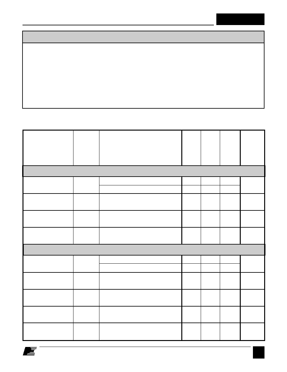
INT200
Conditions
Parameter
Symbol
(Unless Otherwise Specified)
Min
Typ
Max
Units
V
DD
= 15 V, COM = 0V
T
A
= -40 to 85
∞
C
V
IH
= 4.0 V
V
IL
= 1.0 V
1 Suffix
2 Suffix
V
HSD1
, V
HSD2
= 500 V
V
HSD1
, V
HSD2
= 10 V
V
HSD1
, V
HSD2
= 25 V
0
10
150
-20
0
20
4.0
1.0
0.3
0.7
600
700
800
900
0.1
15
5
25
156
10
I
IH,
I
IL
V
IH
V
IL
V
HY
BV
DSS
I
HSD(OFF)
I
HSD(ON)
t
HSD(ON)
C
OSS
µ
A
V
V
V
V
µ
A
mA
ns
pF
HSD OUTPUTS
HSD1/HSD2 Voltage (1 Suffix) ................................. 600 V
(2 Suffix) ................................. 800 V
HSD1/HSD2 Slew Rate ........................................... 10 V/ns
V
DD
Voltage ................................................................ 16.5 V
Logic Input Voltage ...................................... -0.3V to 5.5 V
LS OUT Voltage ................................ -0.3 V to V
DD
+ 0.3 V
Storage Temperature ....................................... ≠65 to 125
∞
C
Ambient Temperature ........................................ -40 to 85
∞
C
Junction Temperature ................................................. 150
∞
C
Lead Temperature
(2)
. ................................................... 260
∞
C
ABSOLUTE MAXIMUM RATINGS
1
Power Dissipation
PF Suffix (T
A
= 25
∞
C) ......................................... 1.25 W
(T
A
= 70
∞
C) ....................................... 800 mW
TF Suffix (T
A
= 25
∞
C) ......................................... 1.04 W
(T
A
= 70
∞
C) ....................................... 667 mW
Thermal Impedance (
JA
)
PF Suffix ........................................................... 100
∞
C/W
TF Suffix ........................................................... 120
∞
C/W
1. Unless noted, all voltages referenced to COM, T
A
= 25
∞
C
2. 1/16" from case for 5 seconds.
LOGIC
Input Current,
High or Low
Input Voltage
High
Input Voltage
Low
Input Voltage
Hysteresis
Breakdown
Voltage
Off-State
Output Current
On-State
Output Current
On-State
Pulse Width
Output
Capacitance
5