
Figure 1. (a) Typical Application ≠ not a Simplified Circuit and
(b) Output Characteristic Tolerance Envelopes.
Product Highlights
Cost Effective Linear/RCC Replacement
∑ Lowest cost and component count, constant voltage (CV)
or constant voltage/constant current (CV/CC) solutions
∑ Optimized for bias winding feedback
∑ Up to 75% lighter power supply reduces shipping cost
∑ Primary based CV/CC solution eliminates 10 to 20
secondary components for low system cost
∑ Fully integrated auto-restart for short circuit and open
loop fault protection ≠ saves external component costs
∑ 42 kHz operation with optimized switching
characteristics for significantly reduced EMI
Much Higher Performance Over Linear/RCC
∑ Universal input range allows worldwide operation
∑ Up to 70% reduction in power dissipation ≠ reduces
enclosure size significantly
∑ CV/CC output characteristic without secondary feedback
∑ System level thermal and current limit protection
∑ Meets all single point failure requirements with only one
additional bias capacitor
∑ Controlled current in CC region provides inherent soft-start
∑ Optional opto feedback improves output voltage accuracy
EcoSmart
Æ
≠ Extremely Energy Efficient
∑ Consumes <300 mW at 265 VAC input with no load
∑ Meets California Energy Commission (CEC), Energy
Star, and EU requirements
∑ No current sense resistors ≠ maximizes efficiency
Applications
∑ Linear transformer replacement in all 3 W applications
∑ Chargers for cell phones, cordless phones, PDAs, digital
cameras, MP3/portable audio devices, shavers, etc.
∑ Home appliances, white goods and consumer electronics
∑ Constant output current LED lighting applications
∑ TV standby and other auxiliary supplies
Description
LinkSwitch
is specifically designed to replace low power linear
transformer/RCC chargers and adapters at equal or lower system
cost with much higher performance and energy efficiency.
LNK520 is equivalent to LNK500 but optimized for use with bias
winding feedback and has improved switching characteristics
for significantly reduced EMI. In addition, if bias and output
windings are magnetically well coupled, output voltage load
Table 1.
Notes: 1. Output power for designs in an enclosed adapter
measured at 50 ∞C ambient. 2. See Figure 1 (b) for Min (CV only
designs) and Typ (CV/CC charger designs) power points identified
on output characteristic. 3. Uses higher reflected voltage transformer
designs for increased power capability
≠
see Key Application
Considerations section. 4. For lead-free package options, see Part
Ordering Information.
regulation can be improved. With efficiency of up to 75% and
<300 mW no-load consumption, a LinkSwitch solution can
save the end user enough energy over a linear design to
completely pay for the full power supply cost in less than
one year. LinkSwitch integrates a 700 V power MOSFET,
PWM control, high voltage start-up, current limit, and thermal
shutdown circuitry, onto a monolithic IC.
LNK520
LinkSwitch
Æ
Family
Energy Efficient, CV or CV/CC Switcher for
Very Low Cost Adapters and Chargers
February 2005
+
PI-3577-080603
Min
(CV only)
Example Characteristic
Typ
(CV/CC)
(a)
(b)
For Circuit
Shown Above
With Optional
Secondary Feedback**
*Estimated tolerance achievable in high volume production (external
components with
±7.5% transformer inductance tolerance included).
**See Optional Secondary Feedback section.
±10%
±24%*
±5%
±24%*
I
O
I
O
V
O
V
O
DC
Output
(V
O
)
Wide Range
HV DC Input
S
D
C
LinkSwitch
PI-3853-030404
OUTPUT POWER TABLE
1
PRODUCT
4
230 VAC ±15% 85-265 VAC No-Load
Input
Power
Min
2
Typ
2
Min
2
Typ
2
LNK520
P or G
3.3 W
4 W 2.4 W 3 W <300 mW
4.2 W 5.5 W 2.9 W 3.5 W <500 mW
3
2
LNK520
E
2/05
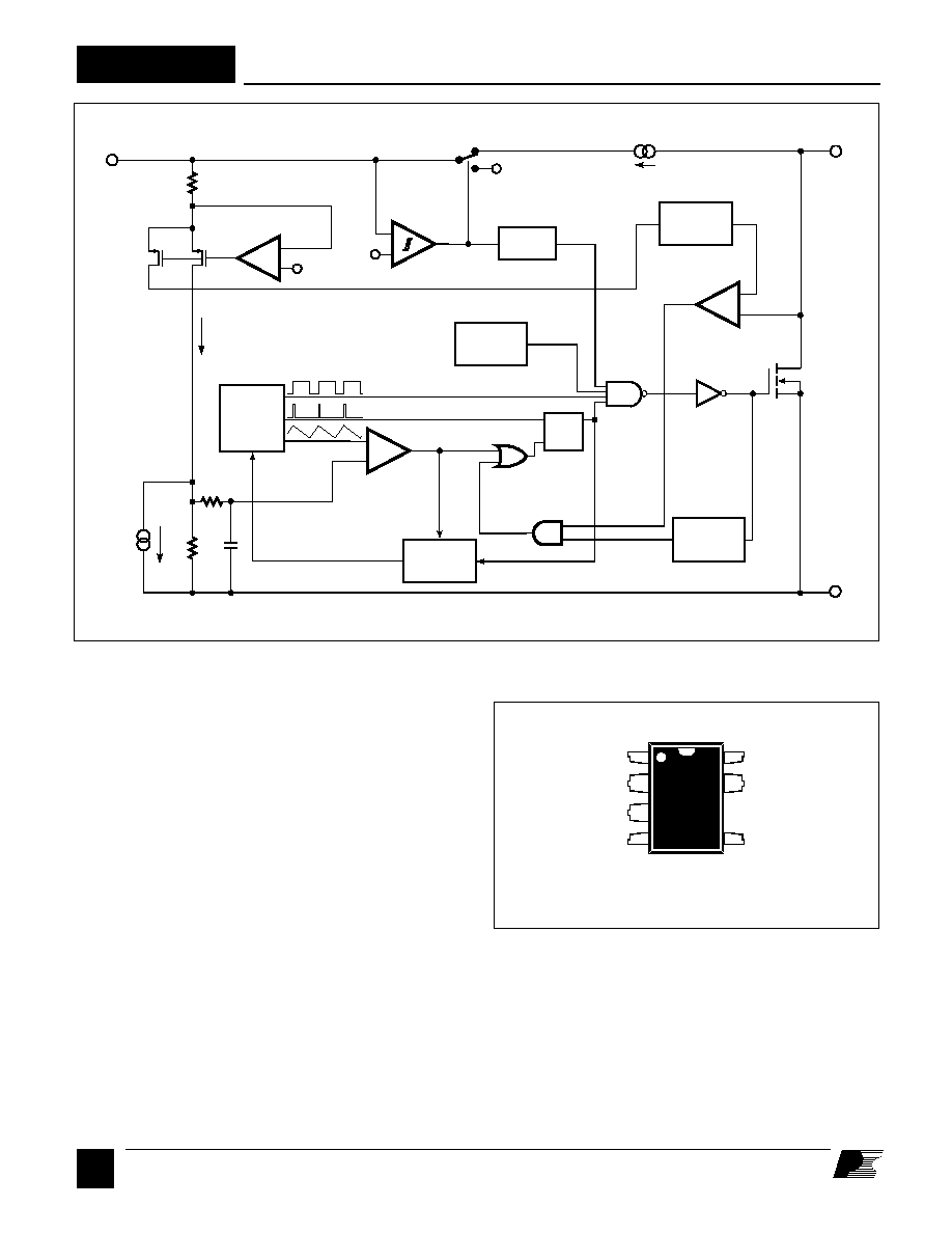
Pin Functional Description
DRAIN (D) Pin:
Power MOSFET drain connection. Provides internal operating
current for start-up. Internal current limit sense point for drain
current.
CONTROL (C) Pin:
Error amplifier and feedback current input pin for duty cycle
and current limit control. Internal shunt regulator connection
to provide internal bias current during normal operation. It is
also used as the connection point for the supply bypass and
auto-restart/compensation capacitor.
SOURCE (S) Pin:
Output MOSFET source connection for high voltage power
return. Primary side control circuit common and reference
point.
Figure 3. Pin Configuration.
Figure 2. Block Diagram.
PI-2777-032503
SHUTDOWN/
AUTO-RESTART
PWM
COMPARATOR
CLOCK
SAW
OSCILLATOR
INTERNAL
SUPPLY
5.6 V
4.7 V
SOURCE
S
R
Q
DMAX
-
+
CONTROL
-
+
5.6 V
I
FB
Z C
VC
+
-
EDGE
0
1
HYSTERETIC
THERMAL
SHUTDOWN
LEADING
EDGE
BLANKING
CURRENT
LIMIT
ADJUST
LOW
FREQUENCY
OPERATION
SHUNT REGULATOR/
ERROR AMPLIFIER
+
-
DRAIN
IDCS
CURRENT LIMIT
COMPARATOR
RE
˜ 8
PI-3790-121503
S
D
S
S
S
C
5
7
8
S
4
2
3
1
P Package (DIP-8B)
G Package (SMD-8B)
LNK520
3
LNK520
E
2/05
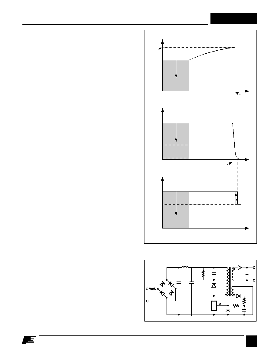
Figure 4. CONTROL Characteristics.
Figure 5. Power Supply Schematic outline.
PI-3579-031004
Internal Current Limit
CONTROL Current
I
C
I
DCS
CONTROL Current
I
C
CONTROL Current
I
C
Duty Cycle
Frequency
I
LIM
I
DCT
77%
30%
3.8%
f
OSC
f
OSC(low)
Auto-restart
Auto-restart
Auto-restart
I
CD1
V
OUT
V
IN
S
D
C
D3
R3
C4
D1
D2
C3
C1
I
C
LinkSwitch
PI-3578-021405
R1
C2
R2
LinkSwitch
Functional Description
The duty cycle, current limit and operating frequency
relationships with CONTROL pin current are shown in
Figure 4. Figure 5 shows a typical power supply schematic outline
which is used below to describe the LinkSwitch operation.
Power Up
During power up, as V
IN
is first applied (Figure 5), the CONTROL
pin capacitor C1 is charged through a switched high voltage
current source connected internally between the DRAIN and
CONTROL pins (see Figure 2). When the CONTROL pin voltage
reaches approximately 5.6 V relative to the SOURCE pin, the
high voltage current source is turned off, the internal control
circuitry is activated and the high voltage internal MOSFET
starts to switch. At this point, the charge stored on C1 is used
to supply the internal consumption of the chip.
Constant Current (CC) Operation
As the output voltage, and therefore the reflected voltage across
the transformer bias winding ramp up, the feedback CONTROL
current I
C
flowing through R1 increases. As shown in Figure 4,
the internal current limit increases with I
C
and reaches I
LIM
when
I
C
is equal to I
DCT
. The internal current limit vs. I
C
characteristic
is designed to provide an approximately constant power supply
output current as the power supply output voltage rises.
Constant Voltage (CV) Operation
When I
C
exceeds I
DCS
, typically 2 mA (Figure 4), the maximum
duty cycle is reduced. At a value of I
C
that depends on power
supply input voltage, the duty cycle control limits LinkSwitch
peak current below the internal current limit value. At this point
the power supply transitions from CC to CV operation. With
minimum input voltage in a typical universal input design, this
transition occurs at approximately 30% duty cycle. Resistor R1
(Figure 5) is therefore initially selected to conduct a value of I
C
approximately equal to I
DCT
when V
OUT
is at the desired value
at the minimum power supply input voltage. The final choice
of R1 is made when the rest of the circuit design is complete.
When the duty cycle drops below approximately 4%, the
frequency is reduced, which reduces energy consumption under
light load conditions.
Auto-Restart Operation
When a fault condition, such as an output short circuit or open
loop, prevents flow of an external current into the CONTROL
pin, the capacitor C1 discharges towards 4.7 V. At 4.7 V, auto-
restart is activated, which turns the MOSFET off and puts the
control circuitry in a low current fault protection mode. In
auto-restart, LinkSwitch periodically restarts the power supply
so that normal power supply operation can be restored when
the fault is removed.

4
LNK520
E
2/05
LNK520
LinkSwitch
85-265
VAC
V
OUT
RTN
C3
C4
C2
C1
C
S
D
R3
R2
R5
R4
R1
D2
D1
VR1
D3
PI-3703-030404
U1
T1
Figure 6. Power Supply Schematic Outline with Optocoupler Feedback, Providing Tight CV Regulation.
The characteristics described above provide an approximate
CV/CC power supply output without the need for secondary side
voltage or current feedback. The output voltage regulation is
influenced by how well the voltage across C2 tracks the reflected
output voltage. This tracking is influenced by the coupling
between transformer output and bias windings. Tight coupling
improves CV regulation and requires only a low value for resistor
R2. Poor coupling degrades CV regulation and requires a higher
value for R2 to filter leakage inductance spikes on the bias
winding voltage waveform. This circuitry, used with standard
transformer construction techniques, provides much better
output load regulation than a linear transformer, making this an
ideal power supply solution in many low power applications.
If even tighter load regulation is required, an optocoupler
configuration can be used while still employing the constant
output current characteristics provided by LinkSwitch.
Optional Secondary Feedback
Figure 6 shows a typical power supply schematic outline using
LinkSwitch
with optocoupler feedback to improve output voltage
regulation. On the primary side, the schematic only differs
from Figure 5 by the addition of optocoupler U1 transistor in
parallel to R1.
On the secondary side, the addition of voltage sense circuit
components R4, VR1 and U1 LED provide the voltage feedback
signal. In the example shown, a simple Zener (VR1) reference
is used though more accurate references may be employed for
improved output voltage tolerancing and to provide cable drop
compensation, if required. Resistor R4 provides biasing for VR1.
The regulated output voltage is equal to the sum of the VR1
Zener voltage plus the forward voltage drop of the U1 LED.
Resistor R5 is an optional low value resistor to limit U1 LED
peak current due to output ripple. Manufacturers specifications
for U1 current and VR1 slope resistance should be consulted
to determine whether R5 is required.
When the power supply operates in the constant current (CC)
region, for example at start up and when charging a battery,
the output voltage is below the voltage feedback threshold
defined by U1 and VR1 and the optocoupler is fully off. In this
region, the circuit behaves exactly as previously described with
reference to Figure 5 where the voltage across C2 and therefore
the current flowing through R1 increases with increasing output
voltage and the LinkSwitch internal current limit is adjusted to
provide an approximate CC output characteristic.
When the output reaches the voltage feedback threshold set by
U1 and VR1, the optocoupler turns on. Any further increase
in the power supply output voltage results in the U1 transistor
current increasing. The resulting increase in the LinkSwitch
CONTROL current reduces the duty cycle according to
Figure 4 and therefore, maintains the output voltage
regulation.
Figure 7 shows the influence of optocoupler feedback on the
output characteristic. The envelope defined by the dashed lines
represent the worst-case power supply DC output voltage and
current tolerances (unit-to-unit and over the input voltage range)
if an optocoupler is not used. A typical example of an inherent
(without optocoupler) output characteristic is shown dotted.
This is the characteristic that would result if U1, R4, R5 and
VR1 were removed. The optocoupler feedback results in the
characteristic shown by the solid line. The load variation arrow in
Figure 7 represents the locus of the output characteristic normally
seen during a battery charging cycle. The two characteristics
are identical as the output voltage rises but then separate as
shown when the voltage feedback threshold is reached. This

5
LNK520
E
2/05
Output Voltage
Tolerance envelope
without optocoupler
Inherent
CC to CV
transition
point
Load variation
during battery
charging
Voltage
feedback
threshold
Characteristic with
optocoupler
Typical inherent
characteristic without
optocoupler
PI-2788-092101
Output Current
Output Voltage
Output Current
V
O(MAX)
Tolerance envelope
without optocoupler
Characteristic with
optocoupler
Power supply peak
output power curve
Typical inherent
characteristic without
optocoupler
PI-2790-112102
Inherent
CC to CV
transition
point
Load variation
during battery
charging
Characteristic observed with
load variation often applied during
laboratory bench testing
Voltage
feedback
threshold
Figure 7. Influence of the Optocoupler on the Power Supply Output Characteristic.
Figure 8. Output Characteristic with Optocoupler Regulation (Reduced Voltage Feedback Threshold).
is the characteristic seen if the voltage feedback threshold is
above the output voltage at the inherent CC to CV transition
point also indicated in Figure 7.
Figure 8 shows a case where the voltage feedback threshold
is set below the voltage at the inherent CC to CV transition
point. In this case, as the output voltage rises, the secondary
feedback circuit takes control before the inherent CC to CV
transition occurs. In an actual battery charging application, this
simply limits the output voltage to a lower value. However, in
laboratory bench tests, it is often more convenient to test the
power supply output characteristic starting from a low output
current and gradually increasing the load. In this case, the
optocoupler feedback regulates the output voltage until the
peak output power curve is reached as shown in Figure 8. Under
these conditions, the output current will continue to rise until the
peak power point is reached and the optocoupler turns off. Once
the optocoupler is off, the CONTROL pin feedback current is
determined only by R1 and the output current therefore folds
back to the inherent CC characteristic as shown. Since this type
of load transition does not normally occur in a battery charger,
the output current never overshoots the inherent constant current
value in the actual application.
In some applications it may be necessary to avoid any output
current overshoot, independent of the direction of load variation.