 | –≠–ª–µ–∫—Ç—Ä–æ–Ω–Ω—ã–π –∫–æ–º–ø–æ–Ω–µ–Ω—Ç: RD5 | –°–∫–∞—á–∞—Ç—å:  PDF PDF  ZIP ZIP |
RD5
85 to 265 VAC Input, 20W (30W Peak) Output
Product Highlights
Low Cost Production Worthy Reference Design
∑ Only 22 components!
∑ Single sided board
∑ Low cost thru-hole components
∑ Fully assembled and tested
∑ Easy to evaluate and modify
∑ Extensive performance data
∑ Up to 80% efficiency
∑ Light weight ≠ no heat sink required for TOPSwitch-II
Fully Protected by
TOPSwitch-II
∑ Primary safety current limit
∑ Output short circuit protection
∑ Thermal shutdown protects entire power supply
Designed for World Wide Operation
∑ Designed for IEC/UL safety requirements
∑ Meets VDE Class B EMI specifications
Description
The RD5 reference design board is an example of a very low
cost production worthy power supply design using the
TOPSwitch family of Three-terminal Off-line PWM Switchers
from Power Integrations. It is intended to help TOPSwitch
users to develop their products quickly by providing a basic
design that can be easily modified to fit a particular application.
In most cases, a minor change to the transformer for a different
output voltage is all that is needed. Multiple output voltages are
obtained just as easily. A constant current or constant power
output may be implemented with the addition of a few low cost
components.
Typical applications include AC-DC adapters for laptops,
notebooks and PDAs, battery chargers for cellular telephones,
power tools and camcorders, VTR/VCR, video game, appliance
and satellite decoder power supplies.
Æ
Reference Design Board
TOPSwitch-II
Æ
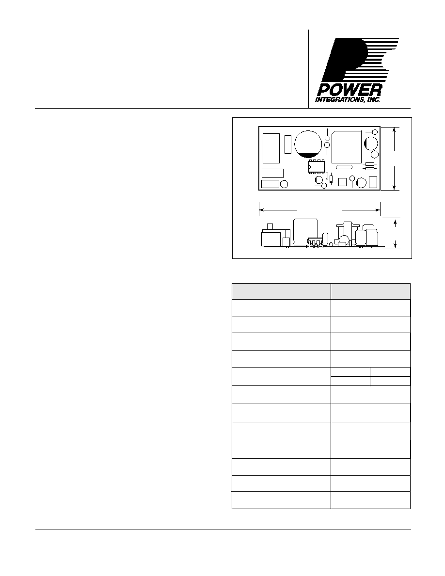
Figure 1. RD5 Board Overall Physical Dimensions.
Figure 2. Table of Key Electrical Parameters.
o
VDE B
(VFG243 B)
CISPR22
Efficiency
78%
PARAMETER
LIMITS
Input Voltage Range
85 to 265 VAC
Input Frequency Range
47 to 440 Hz
Temperature Range
0 to 50
∞
C
Output Voltage
(I = 1.0A)
12 V
±
5%
Output Power
(continuous)
Output Power
(peak)
30W
Line Regulation
(85-265 VAC)
±
1%
Load Regulation
(10%-100%)
±
1%
Output Ripple Voltage
±
60 mV MAX
Safety
IEC 950 / UL1950
EMI
50∞C 15W
25∞C 20W
PI-2058-041698
1.06 in.
(27 mm)
1.69 in.
(43 mm)
3.57 in. (91 mm)
July 1997
RD5
A
7/97
34
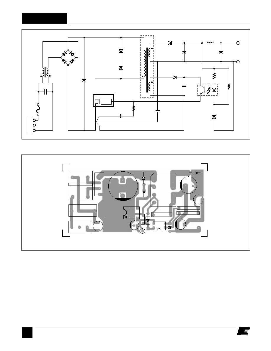
Figure 4. Component Legend of the RD5.
General Circuit Description
The RD5 is a low-cost, flyback switching power supply using
the TOP224P integrated circuit. The circuit shown in Figure 3
produces a 12 V, 20 W power supply that operates from 85 to
265 VAC input voltage. The 12 V output is directly sensed by
optocoupler U2 and Zener diode VR2. The output voltage is
determined by the Zener diode (VR2) voltage and the voltage
drops across the optocoupler (U2) LED and resistor R1. Other
output voltages are also possible by adjusting the transformer
Figure 3. Schematic Diagram of the 12V RD5 Power Supply.
PI-2053-041698
D2
50SQ100
D3
1N4148
C2
560
µ
F
35 V
C3
220
µ
F
35 V
T1
D1
UF4005
VR1
P6KE200
VR2
1N5241B
11 V
R2
150
BR1
600 V
C1
47
µ
F
400 V
F1
3.15 A
J1
C6
0.1
µ
F
250 VAC
L2
19 mH
L
N
C5
47
µ
F
U1
TOP224P
D
S
C
CONTROL
TOPSwitch-II
R3
6.8
L1
3.3
µ
H
C4
0.1
µ
F
U2
PC817A
R1
39
C7
1 nF
250 VAC
Y1
+12V
RTN
1
2
4
3
5, 6
7, 8
L1
C2
J2
R2
R1
C3
T1
U2
D2
D3
C7
VR1
C4
C5
U1
F1
L2
BR1
D1
PI-2059-062697
COMPONENT SIDE SHOWN
+
J1
VR2
C6
C1
POWER
INC.
INTEGRATIONS
RD5
Rev. A
S/N
R3
turns ratios and value of Zener diode VR2.
AC power is rectified and filtered by BR1 and C1 to create the
high voltage DC bus applied to the primary winding of T1. The
other side of the transformer primary is driven by the integrated
high-voltage MOSFET within the TOP224. D1 and VR1
clamp the leading-edge voltage spike caused by transformer
leakage inductance to a safe value and reduce ringing. The

A
7/97
RD5
35
Component Listing
Reference
Value
Part Number
Manufacturer
BR1
600 V, 2 A
2KBPC06M
General Instrument
C1
47
µ
F, 400 V
381LX470M400H012
Cornell-Dubilier
C2
560
µ
F, 35 V
ECA-1VFQ561
Panasonic
C3
220
µ
F, 35 V
ECE-A1VGE221
Panasonic
C4
0.1
µ
F, 50 V
RPE131R104M50
Murata
C5
47
µ
F, 10 V
ECE-A1AG470
Panasonic
C6
0.1
µ
F, 250 VAC, X
F1772-410-2000
Roederstein
C7*
1.0 nF, 400 VAC, Y1*
DE1110E102M ACT4K-KD Murata
(or WKP102MCPE.OK
Roederstein)
(or PME294RB4100M
Rifa)
D1
600 V, 1A, UFR
UF4005
General Instrument
D2
100 V, 5A, Schottky
50SQ100
International Rectifier
D3
75 V, Switching
1N4148
National Semiconductor
L1
3.3
µ
H, 6.5 A
622LY-3R3M
Toko
L2
19 mH, 400 mA
ELF15N005A
Panasonic
R1
39
, 1/4 W
5043CX39R00J
Philips
R2
150
, 1/4 W
5043CX150R0J
Philips
R3
6.8
, 1/4 W
5043CX6R800J
Philips
T1**
TRD5
Custom
U1
TOP224P
Power Integrations
U2
PC817A
Sharp
VR1
200 V Zener TVS
P6KE200
General Instrument
VR2
11 V Zener
1N5241B
Motorola
F1
3.15 A, 250 VAC
19372K, 3.15A
Wickman
Figure 5. Parts List for the RD5 (* Two Series Connected, 2.2 nF, Y2-Capacitors Such as Murata DE7100F222MVA1-KC can replace C7).
** T1 is available from Premier Magnetics (714) 362-4211 as P/N POL-12017, and from Coiltronics (561) 241-7876 as P/N CTX00-13742.
power secondary winding is rectified and filtered by D2, C2,
L1, and C3 to create the 12 V output voltage. R2 and VR2
provide a slight pre-load on the 12 V output to improve load
regulation at light loads. R2 also provides bias current for Zener
VR2 to improve regulation. The bias winding is rectified and
filtered by D3 and C4 to create a bias voltage to the TOP224P.
L2 and Y1-capacitor C7 attenuate common-mode emission
currents caused by high-voltage switching waveforms on the
DRAIN side of the primary winding and the primary to secondary
capacitance. L2 and C6 attenuate differential-mode emission
currents caused by the fundamental and harmonics of the
primary current waveform. C5 filters internal MOSFET gate
drive charge current spikes on the CONTROL pin, determines
the auto-restart frequency, and together with R1 and R3,
compensates the control loop.
The circuit performance data shown in Figures 6-18 were
measured with AC voltage applied to the RD5.
Load Regulation (Figure 6) ≠ The amount of change in the DC
output voltage for a given change in output current is referred
to as load regulation. The 12 V output stays within
±
1% from
10% to 100% of rated load current. The TOPSwitch on≠chip
overtemperature protection circuit will safely shut down the
power supply under persisting overload conditions. Below
minimum load, the 12 V output rises slightly due to the
TOPSwitch minimum duty cycle.
Line Regulation (Figure 7) - The amount of change in the DC
output voltage for a given change in the AC input voltage is
called line regulation. The maximum change in output voltage
is within
±
1%.
Efficiency (Line Dependent) ≠ Efficiency is the ratio of the
output power to the input power. The curves in Figures 8 and 9
show how the efficiency changes with input voltage.
Efficiency (Load Dependent) ≠ The curves in Figures 10 and 11
show how the efficiency changes with output power for 115
VAC and 230 VAC inputs.
Power Supply Turn On Sequence ≠ The internal switched, high-
voltage current source provides the initial bias current for
TOPSwitch when power is first applied. The waveforms shown
RD5
A
7/97
36
General Circuit Description (cont.)
Figure 6. Load Regulation
Figure 7. Line Regulation
Load Current (A)
Output Voltage (% of Nominal)
PI-2062-070297
0
0.5
1
1.5
100
100
90
90
110
110
Load Current (A)
0
0.5
1
1.5
VIN = 115 VAC
VIN = 230 VAC
2
2
Input Voltage (VAC)
Output Voltage (% of Nominal)
PI-2063-070297
50
100
150
200
250
300
100
IL = 0.33 A
100
90
90
IL = 1.67 A
110
110
Input Voltage (VAC)
50
100
150
200
250
300
15 W output is outlined on the non-component side of the board,
and is approximately 0.56 in
2
(3.6 cm
2
). The RD5 printed circuit
board utilizes 2 oz. copper cladding. Printed circuit boards with
lighter cladding will require apertures in the solder mask to
build-up effective trace thickness.
Transformer Specification
The electrical specifications and construction details for
transformer TRD5 are shown in Figures 19 and 20. Transformer
TRD5 is supplied with the RD5 reference design board. This
design utilizes an EI25 core and a triple insulated wire secondary
winding. The use of triple insulated wire allows the transformer
to be constructed using a smaller core and bobbin than a
conventional magnet wire design due to the elimination of the
margins required for safety spacing in a conventional design.
If a conventional margin wound transformer is desired, the
design of Figures 21-22 can be used. This design (TRD5-1)
uses a EEL22 core and bobbin to accommodate the 3 mm
margins required to meet international safety standards when
using magnet wire rather than triple insulated wire, and has the
same pinout and printed circuit foot print as TRD5. The
transformer is approximately 50% taller than the triple insulated
wire design due to the inclusion of creepage margins required
to meet international safety standards.
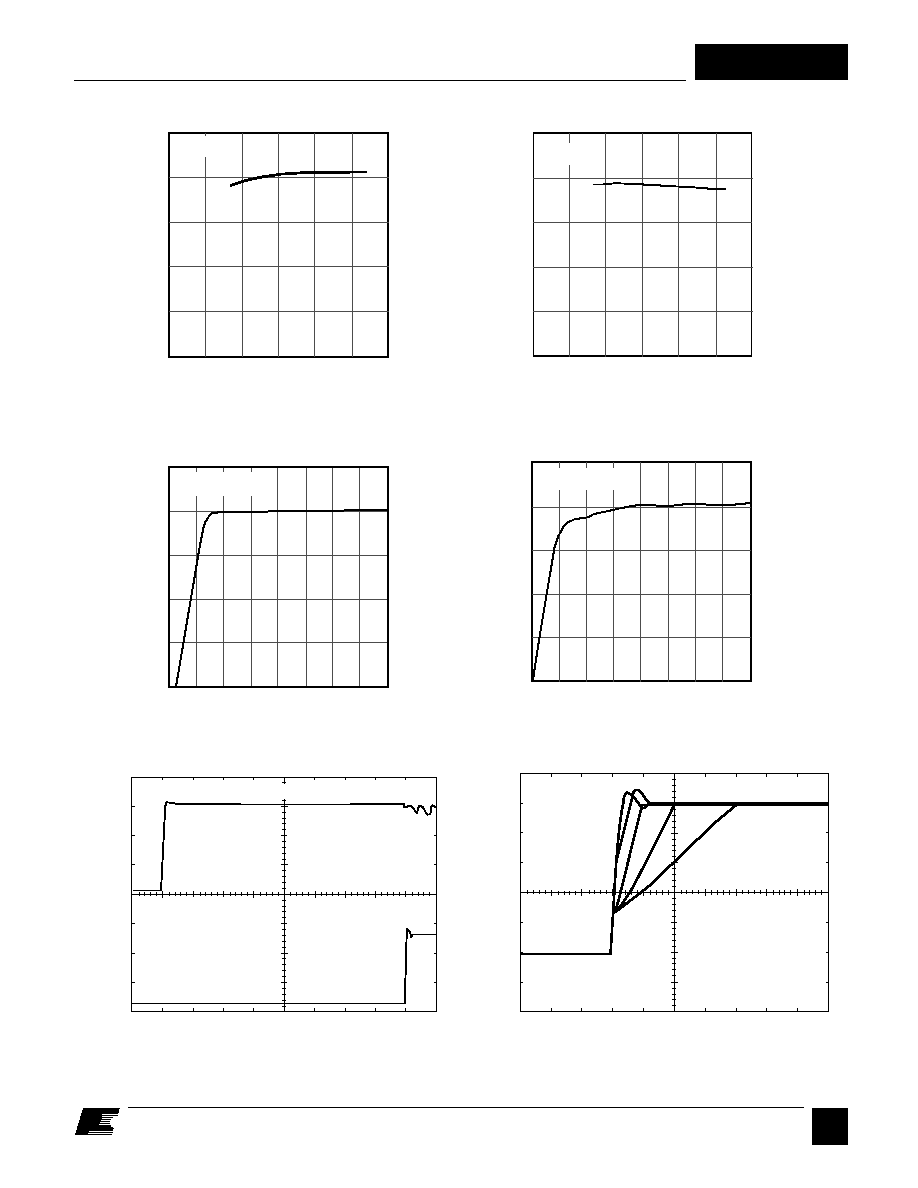
in Figure 12 illustrate the relationship between the high-voltage
DC bus and the 12 V output voltage. Capacitor C1 charges to
the peak of the AC input voltage before TOPSwitch turns on.
The delay of 160 ms (typical) is caused by the time required to
charge the auto-restart capacitor C5 to 5.8 V. At this point the
power supply turns on as shown.
Figure 13 shows the output voltage turn on transient as well as
a family of curves associated with an additional soft-start
capacitor. The soft-start capacitor is placed across VR2 and can
range in value from 4.7 uF to 47 uF as shown.
Line frequency ripple voltage is shown in Figure 14 for 115
VAC input and 20 W output. Switching frequency ripple
voltage is shown in Figure 15 for the same test condition.
The power supply transient response to a step load change from
1.25 to 1.67 A (75% to 100%) is shown in Figure 16. Note that
the response is quick and well damped.
The RD5 is designed to meet worldwide safety and EMI (VDE
B) specifications. Measured conduction emissions are shown
in Figure 17 for 115 VAC and Figure 18 for 230 VAC.
Thermal Considerations
The RD5 utilizes the printed circuit copper for TOPSwitch
heatsinking. For 20 W output, the heatsink area is approximately
1.25 in
2
(8 cm
2
). The copper area required for heatsinking at
A
7/97
RD5
37
Figure 12. Turn On Delay
Figure 13. Output Voltage Turn On Transient vs. Soft Start Capacitor
Figure 8. Efficiency vs. Input Voltage, 20 W Output
Figure 9. Efficiency vs. Input Voltage, 4 W Output
Figure 10. Efficiency vs. Output Power, 115 VAC Input
Figure 11. Efficiency vs. Output Power, 230 VAC Input
0
0
100
300
200
Input Voltage (VAC)
Output Efficiency (%)
PI-2064-070297
100
Po = 20 W
80
60
40
20
0
0
100
300
200
Input Voltage (VAC)
Output Efficiency (%)
PI-2065-070297
100
Po = 4 W
80
60
40
20
PI-2068-070297
0
100
200
Time (ms)
0
5
10
50
0
100
150
15
OUTPUT
VOLTAGE
DC BUS VOLTAGE
PI-2069-070297
0
10
20
Time (ms)
0
6
4
8
10
2
0
µ
F
4.7
µ
F
10
µ
F 22
µ
F
47
µ
F
Output Voltage (V)
0
0
10
20
15
5
Output Power (W)
Output Efficiency (%)
PI-2066-070297
100
VIN = 115 VAC
80
60
40
20
0
0
10
20
15
5
Output Power (W)
Output Efficiency (%)
PI-2067-070297
100
VIN = 230 VAC
80
60
40
20