 | –≠–ª–µ–∫—Ç—Ä–æ–Ω–Ω—ã–π –∫–æ–º–ø–æ–Ω–µ–Ω—Ç: RD6 | –°–∫–∞—á–∞—Ç—å:  PDF PDF  ZIP ZIP |

Output Voltage
(I = 3.0 A)
(I = 0.1 A)
o
RD6
85 to 265 VAC Input, 15W Output
Product Highlights
Low Cost Production Worthy Reference Design
∑ Complete self-powered USB power supply
∑ Supports 4 ports and hub controller
∑ Single sided board
∑ Fully assembled and tested
∑ Easy to evaluate and modify
∑ Extensive performance data
∑ Over 69% efficiency
Fully Protected by TOPSwitch-II
∑ Primary safety current limit
∑ Output short circuit protection
∑ Thermal shutdown protects entire supply
Designed for World Wide Operation
∑ Designed for IEC/UL safety requirements
∑ Meets VDE Class B EMI specifications
Description
The RD6 reference design board is an example of a low cost
production worthy design for a self-powered, 4-port USB hub.
The design is a complete solution for powering hubs found in
products such as monitors and printers. A total of 15 W of
power is delivered through two outputs. The main output
supplies 3 A at 5 V. This meets the USB specification of
500 mA for each port (4 port total) with additional power
available for a 5 V hub controller. A second 3.3 V (100 mA)
output provides power for low voltage hub controllers.
The RD6 utilizes the TOP223Y member of the TOPSwitch-II
family of Three-terminal Off-line PWM Switchers from
Power Integrations. It is intended to help TOPSwitch users to
develop their products quickly by providing a production
ready design which needs little or no modification to meet
system requirements.
Æ
USB Reference Design Board
TOPSwitch-II
March 1998
Æ
Figure 1. RD6 Overall Physical Dimensions.
Figure 2. Table of Key Electrical Parameters.
o
VDE B
(VFG243 B)
CISPR22
Efficiency
69% (min)
5 V
±
4%
3.3 V
±
3%
5V
±
40 mV MAX
3.3V
±
25 mV MAX
PARAMETER
LIMITS
Input Voltage Range
85 to 265 VAC
Input Frequency Range
47 to 440 Hz
Temperature Range
0 to 70
∞
C
Output Power
(continuous)
15 W
Output Power
(peak)
30 W
Line Regulation
(85-265 VAC)
±
0.7%
Load Regulation
(0%-100%)
±
1.1%
Output Ripple Voltage
Safety
IEC 950 / UL1950
EMI
PI-2167-012098
1.07 in.
(27 mm)
2.13 in.
(54 mm)
4.29 in. (109 mm)
RD6
B
3/98
2
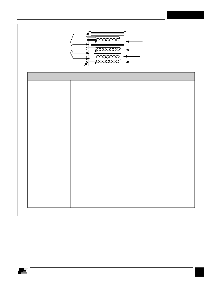
Figure 4. Component Legend of the RD6.
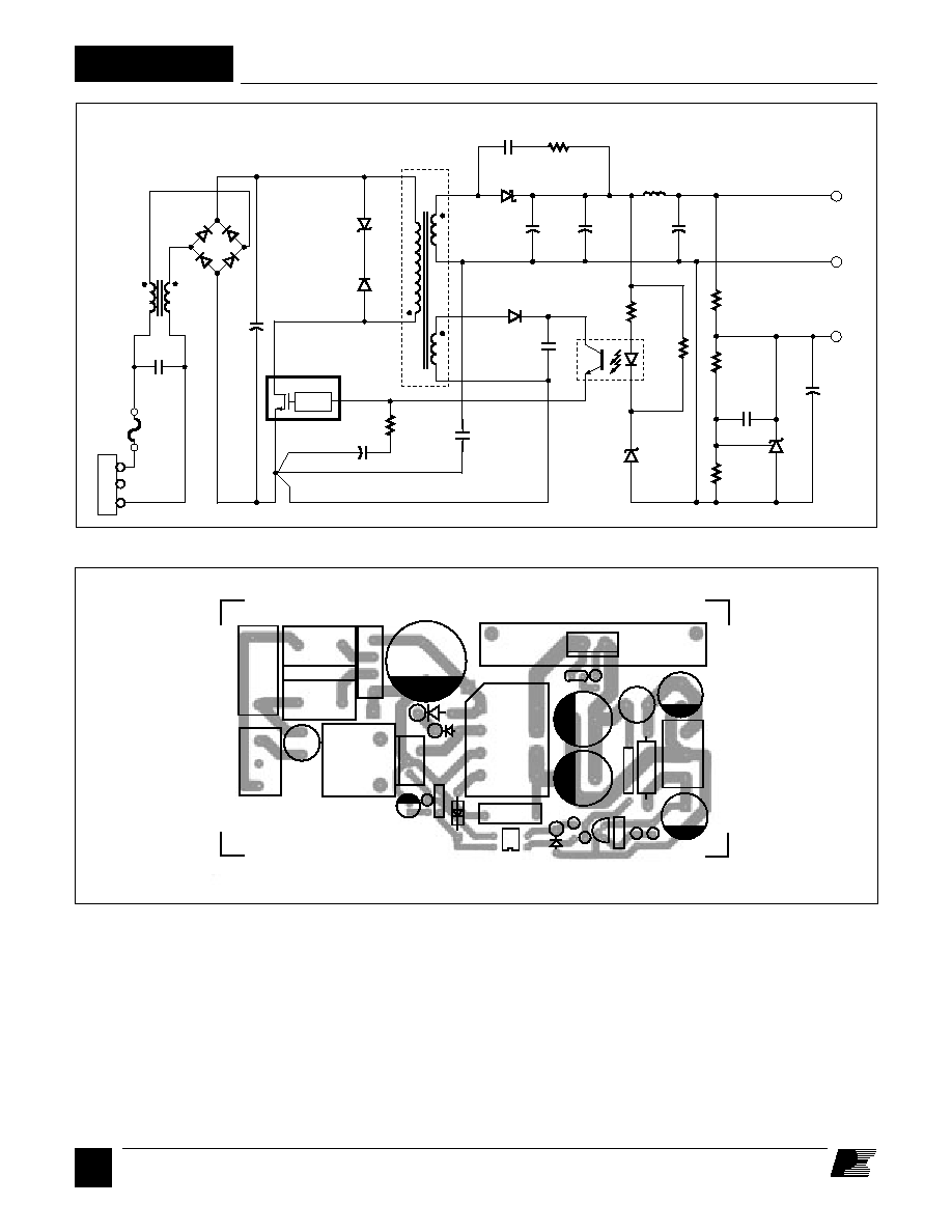
General Circuit Description
The RD6 is a low-cost flyback switching power supply using
the TOP223Y integrated circuit. The circuit shown in Figure 3
details a 5 V, 15 W power supply that operates from 85 to
265 VAC input voltage, suitable for powering a USB hub with
as many as 4 ports, and a 3.3 V, 100 mA auxiliary output for
powering a hub controller. AC power is rectified and filtered
by BR1 and C1 to create the high voltage DC bus applied to the
primary winding of T1. The other side of the transformer
primary is driven by the integrated high-voltage MOSFET
within the TOP223. D1 and VR1 clamp the voltage spike
caused by transformer leakage inductance to a safe value and
reduce ringing. The power secondary winding is rectified and
filtered by D2, C2, C10, L1, and C3 to create the 5 V output
voltage. The 5 V output is directly sensed by optocoupler U2
and Zener diode VR2. The output voltage is determined by the
Zener diode VR2 plus the voltage drops across the LED of the
optocoupler U2 and resistor R1. Other output voltages are also
possible by adjusting the transformer turns ratios and the value
Figure 3. Schematic Diagram of the 15 W RD6 Power Supply.
L1
C9
J2
R12
R1
C3
T1
U2
D2
D3
C7
VR1
C4
C5
U1
F1
BR1
D1
PI-2137-122297
COMPONENT SIDE SHOWN
J1
VR2
C6
C1
RD6 REV. A
POWER INTEGRATIONS INC.
R3
L2
U3 C8
R6
R4
R5
R2
C10
C2
C11
DC-
HS1
S/N
+3.3V GND +5V
PI-2135-030998
D2
MBR1045
D3
1N4148
C2
560
µ
F
35 V
C3
220
µ
F
35 V
T1
D1
UF4005
VR1
P6KE200
VR2
IN5228C
3.9 V
R2
47
BR1
600 V
C1
47
µ
F
400 V
F1
3.15 A
J1
C6
0.1
µ
F
250 VAC
L2
22 mH
L
N
C5
47
µ
F
U1
TOP223Y
D
S
C
CONTROL
TOPSwitch-II
R3
6.8
L1
3.3
µ
H
C4
0.1
µ
F
U2
PC817A
R1
4.7
C7
1 nF
250 VAC
Y1
5 V
RTN
1
2
4
3
5, 6
7, 8
C11
470 pF
R12
15
C10
560
µ
F
35 V
C8
10 nF
R5
10 K
R4
3 K
R6
16
1/2 W
U3
TL431
C9
220
µ
F
35 V
3.3 V

B
3/98
RD6
3
Component Listing
Reference
Value
Part Number
Manufacturer
BR1
600 V, 2 A
2KBPC06M
General Instrument
C1
47
µ
F, 400 V
ECA-2GG470YE
Panasonic
C2, C10
560
µ
F, 35 V
ECA-1VFQ561
Panasonic
C3, C9
220
µ
F, 35 V
ECE-1AVGE221
Panasonic
C4
0.1
µ
F, 50 V
RPE121Z5U104M50V
Murata
C5
47
µ
F, 10 V
ECE-A1AG470
Panasonic
C6
0.1
µ
F, 250 VAC, X2
F1772-410-2000
Roederstein
C7
1.0 nF, 250 VAC, Y1*
WKP102MCPE.OK
Roederstein
DE1110E102M ACT4K-KD Murata
440LD10
Cera-Mite
C8
10 nF, 50 V
RPE110Z5U103M50V
Murata
C11
470 pF, 50 V
RPE110X7R471K50V
Murata
D1
600 V, 1 A, UFR
UF4005
General Instrument
D2
45 V, 10 A Schottky
MBR1045
Motorola
D3
75 V, Switching
1N4148
National Semiconductor
L1
3.3
µ
H, 5.5 A
6000-3R3M
J. W. Miller
L2
22
µ
H, 0.4 A
ELF-18D290C
Panasonic
R1
4.7
, 1/4 W
5043CX4R700J
Philips
R2
47
, 1/4 W
5043CX47R00J
Philips
R3
6.8
, 1/4 W
5043CX6R800J
Philips
R4
3.16 K
, 1/4 W, 1%
5043EM3K160F
Philips
R5
10.0 K
, 1/4 W, 1%
5043EM10K00F
Philips
R6
16
, 1/2 W
5053CX16R00J
Philips
R12
15
, 1/4 W
5043CX15R00J
Philips
T1**
TRD6
Custom
U1
TOP223Y
Power Integrations
U2
Optocoupler, Controlled CTR PC817A
Sharp
U3
Adj. Shunt Regulator
TL431CLP
Motorola
VR1
200 V Zener TVS
P6KE200
Motorola
VR2
3.9 V 2% Zener
1N5228C
APD
F1
3.15 A, 250 VAC
19372, 3.15A
Wickman
Figure 5. Parts List for the RD6 (* Two Series-Connected 2.2 nF, Y2 Capaciors such as Murata P/N DE7100F222MVA1-KC can replace
C7) ** T1 is available from Premier Magnetics (714) 362-4211 as P/N TSD-1106, and from Coiltronics (561) 241-7876 as P/N CTX14-13598
of Zener diode VR2. The 3.3 V output is derived from the 5 V
output using R6 and shunt regulator U3. C11 and R12 form a
snubber circuit across D2 to reduce ringing. This improves
conducted RFI performance of the supply at high frequency
(15-20 MHz) and reduces leakage spikes, improving the
reliability of D2. R2 provides bias current for Zener VR2 to
improve regulation.
The primary bias winding is rectified and filtered by D3 and C4
to create a bias voltage to power the TOP223Y. L2 and
Y1-capacitor C7 attenuate common-mode emission currents
caused by high-voltage switching waveforms on the DRAIN
side of the primary winding and the primary to secondary
capacitance. L2 and C6 attenuate differential-mode emission
currents caused by the fundamental and harmonics of the
primary current waveform. C5 filters internal MOSFET gate
drive charge current spikes on the CONTROL pin, determines
the auto-restart frequency, and together with R1 and R3,
compensates the 5 V control loop. R6 and shunt regulator U3
are used to derive a 3.3 V supply from the 5V output. R4 and
R5, along with the 2.5 V internal band gap reference in U3, are
used to set the output voltage. C8 provides compensation for
the 3.3 V control loop. C9 provides additional filtering for the
3.3 V output. As a shunt regulator, U3 provides a constant load
of approximately 100 mA on the 5 V output, regardless of
whether a load is present on the 3.3 V output. This provides a
substantial preload for the 5 V output, greatly improving
regulation at light or zero load. The circuit performance data
shown in Figures 6-21 were measured with AC voltage applied
to the RD6.
Load Regulation (Figure 6) ≠ The change in the DC output
voltage for a given change in output current is referred to as
load regulation. Both the 5 V and 3.3 V outputs stay within
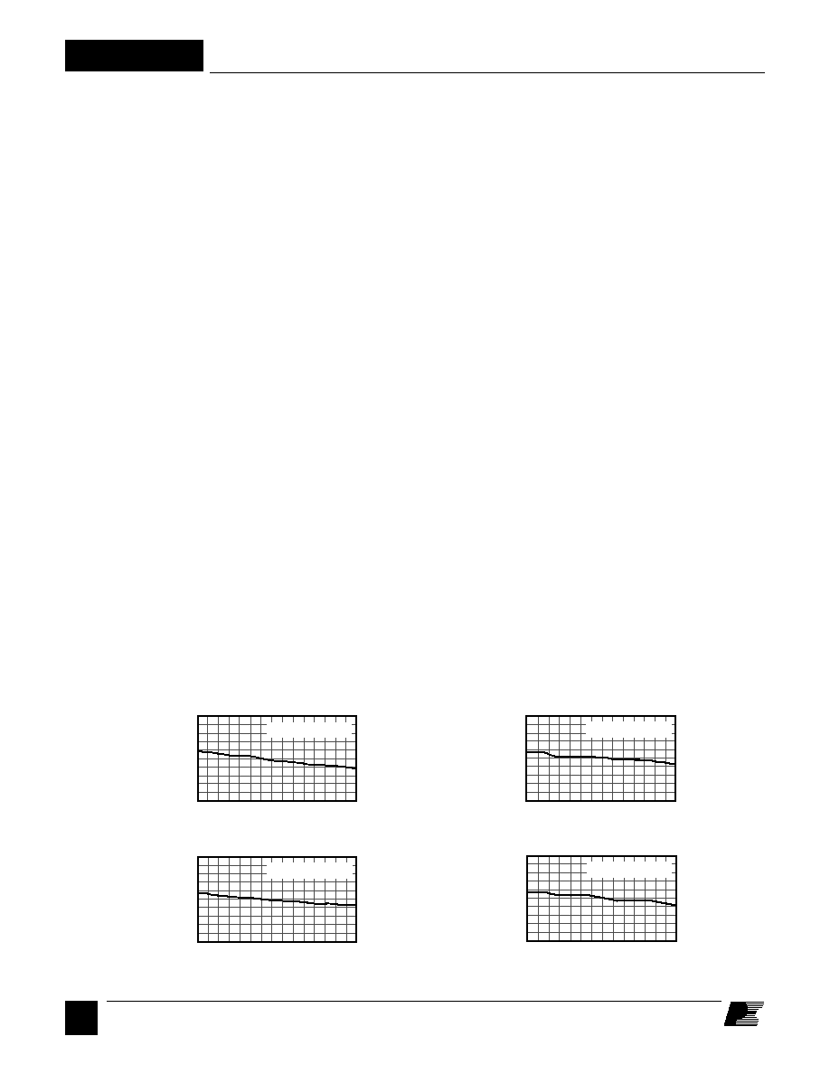
RD6
B
3/98
4
General Circuit Description (cont.)
15 for the same test condition Line frequency and switching
frequency ripple for the 3.3 V output are shown in Figures 17
and 18, respectively.
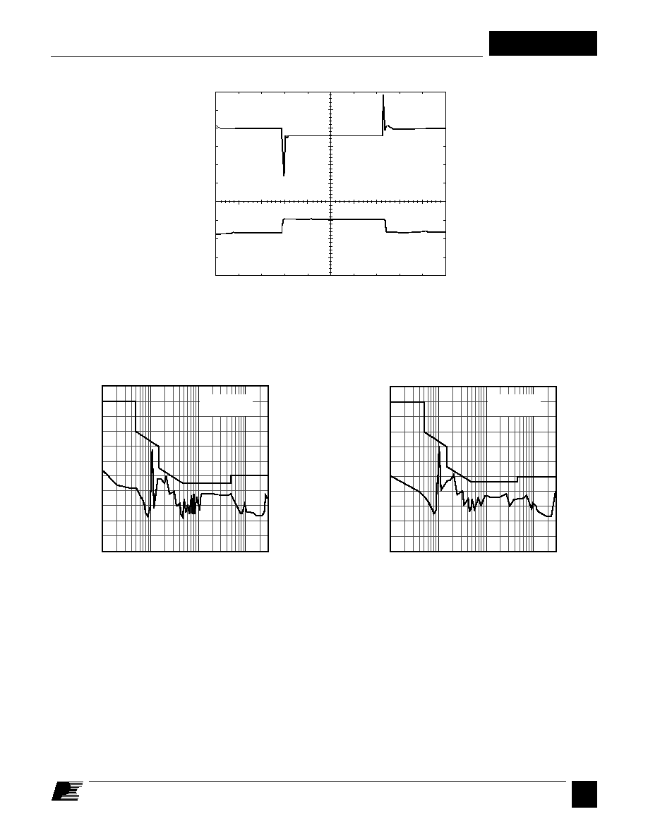
The 5 V output transient response to a step load change from
2.25 to 3 A (75% to 100%) is shown in Figure 19. Note that the
response is quick and well damped. The initial voltage spike in
response to the load step is due to the interaction of the load
current with the ESR of C3. If desired, the amplitude of this
spike can be reduced by substituting a low ESR capcitor for C3.
The RD6 is designed to meet worldwide safety and EMI (VDE
B) specifications. Measured conduction emissions are shown
in Figure 20 for 115 VAC and Figure 21 for 230 VAC.
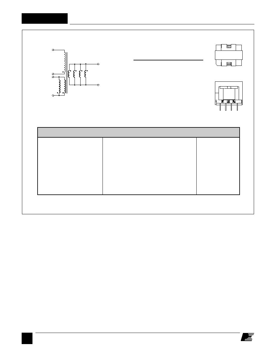
Transformer Specification
The electrical specifications and construction details for
transformer TRD6 are shown in Figures 22 and 23. Transformer
TRD6 is supplied with the RD6 reference design board. This
design utilizes an EI25 core and a triple insulated wire
secondary winding. The use of triple insulated wire allows the
transformer to be constructed using a smaller core and bobbin
than a conventional magnet wire design due to the elimination
of the margins required for safety spacing in a conventional
design.
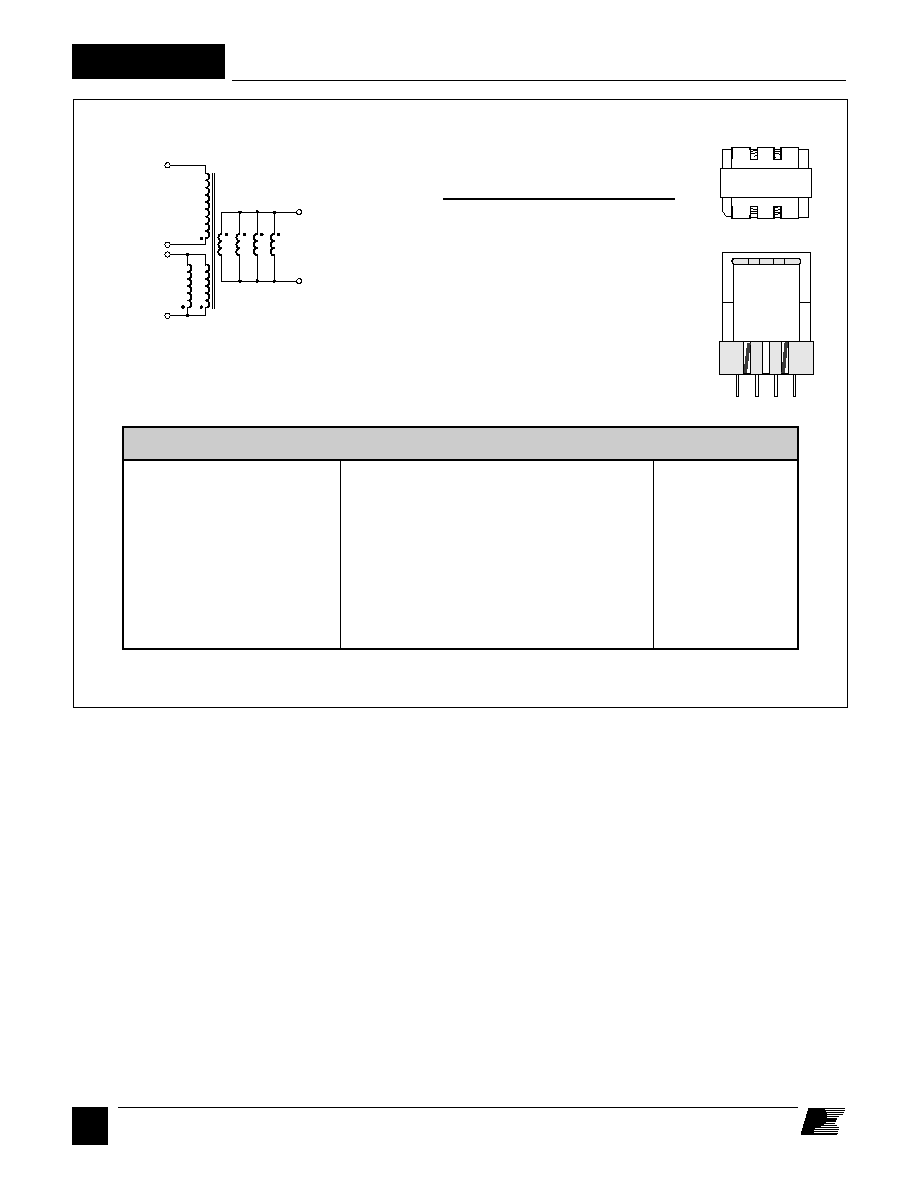
If a conventional margin wound transformer is desired, the
design of Figures 24-25 can be used. This design (TRD6-1)
uses a EEL22 core and bobbin to accommodate the 3 mm
margins required to meet international safety standards when
using magnet wire rather than triple insulated wire, and has the
same pinout and printed circuit foot print as TRD6. The
transformer is approximately 50% taller than the triple
insulated wire design due to the inclusion of creepage margins
required to meet international safety standards.
±
1.1 % of nominal from 0% to 100% of rated load current. The
TOPSwitch on≠chip over-temperature protection circuit will
safely shut down the power supply under persistent overload
conditions.
Line Regulation (Figure 7) - The change in the DC output
voltage for a given change in the AC input voltage is called line
regulation. The maximum change in output voltage vs line for
both the 5 V and 3.3 V outputs is within
±
0.7%.
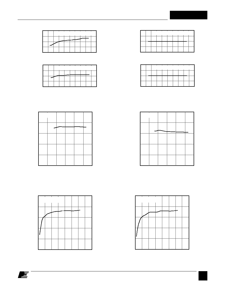
Efficiency (Line Dependent) ≠ Efficiency is the ratio of the
output power to the input power. The curves in Figures 8 and 9
show how the efficiency changes with input voltage.
Efficiency (Load Dependent) ≠ The curves in Figures 10 and
11 show how the efficiency changes with output power for
115 VAC and 230 VAC inputs.
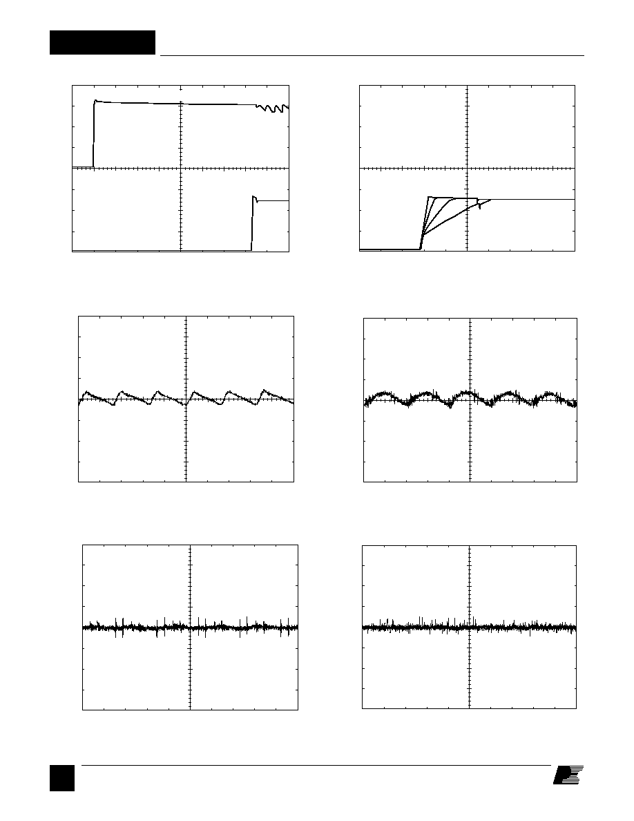
Power Supply Turn On Sequence ≠ The internal switched,
high-voltage current source provides the initial bias current for
TOPSwitch when power is first applied. The waveforms
shown in Figure 12 illustrate the relationship between the
high-voltage DC bus and the 12 V output voltage. Capacitor
C1 charges to the peak of the AC input voltage before TOPSwitch
turns on. The delay of 150 ms (typical) is caused by the time
required to charge the auto-restart capacitor C5 to 5.8 V. At
this point the power supply turns on as shown.
Figure 13 shows the 5 V output turn on transient as well as a
family of curves associated with an additional soft-start
capacitor. The soft-start capacitor is placed across VR2 and
can range in value from 10 uF to 47 uF as shown.
Line frequency ripple voltage for the 5 V output is shown in
Figure 14 for 115 VAC input and 15 W output. Switching
frequency ripple voltage on the 5 V output is shown in Figure
Figure 6. Load Regulation
5V Output Voltage (% of Nominal)
100
95
105
Load Current (A)
0
1.0
2.0
3.0
VIN = 115 VAC
PI-2147-012398
100
95
105
Load Current (A)
0
1.0
2.0
3.0
VIN = 230 VAC
Load Current (A)
3.3V Output Voltage (% of Nominal)
VIN = 115 VAC
0.5
0.1
0
100
95
105
Load Current (A)
VIN = 230 VAC
0.5
0.1
0
100
95
105
B
3/98
RD6
5
Figure 7. Line Regulation
Figure 8. Efficiency vs. Input Voltage, 15.3 W Output
Figure 9. Efficiency vs. Input Voltage, 3 W Output
Figure 10. Output Efficiency vs. Output Power, 115 VAC Input
Figure 11. Output Efficiency vs. Output Power, 230 VAC Input
100
95
105
Input Voltage (VAC)
50
100
150
200
250
300
5V Output Voltage (% of Nominal)
100
95
105
Input Voltage (VAC)
50
100
150
200
250
300
100
95
105
Input Voltage (VAC)
50
100
150
200
250
300
PI-2151-011598
100
95
105
Input Voltage (VAC)
50
100
150
200
250
300
3.3V Output Voltage (% of Nominal)
5V @ 3.0A and 3.3V @ 0.1A
5V @ 3.0A and 3.3V @ 0.1A
5V @ 0.53A and 3.3V @ 0.1A
5V @ 0.53A and 3.3V @ 0.1A
0
0
100
300
200
Input Voltage (VAC)
Output Efficiency (%)
PI-2153-011598
100
Po = 15.3 W
80
60
40
20
0
0
100
300
200
Input Voltage (VAC)
Output Efficiency (%)
PI-2157-011598
100
Po = 3 W
80
60
40
20
0
0
10
20
15
5
Output Power (W)
Output Efficiency (%)
PI-2159-011598
100
VIN = 115 VAC
80
60
40
20
0
0
10
20
15
5
Output Power (W)
Output Efficiency (%)
PI-2161-011598
100
VIN = 230 VAC
80
60
40
20
RD6
B
3/98
6
Figure 12. Turn On Delay
PI-2163-011998
0
100
200
Time (ms)
0
2
4
50
0
100
150
6
OUTPUT
VOLTAGE
DC BUS VOLTAGE
PI-2165-011998
0
100
200
Time (ms)
0
2
4
6
0
µ
F
22
µ
F
10
µ
F
47
µ
F
Output Voltage (V)
Figure 13. Output Voltage Turn On Transient vs Soft Start Capacitor
PI-2169-012098
0
25
50
-40
20
0
40
-20
Output Voltage (mV)
Time (ms)
60
80
-60
-80
PI-2171-012098
0
25
50
-40
20
0
40
-20
Output Voltage (mV)
Time (
µ
s)
60
80
-60
-80
Figure 15. 5 V Switching Frequency Ripple, 115 VAC Input, 15.3 W Output
PI-2173-012098
0
25
50
-40
20
0
40
-20
Output Voltage (mV)
Time (ms)
60
80
-60
-80
PI-2175-012098
0
25
50
-40
20
0
40
-20
Output Voltage (mV)
Time (
µ
s)
60
80
-60
-80
Figure 16. 3.3 V Line Frequency Ripple, 115 VAC Input, 15.3 W Output
Figure 17. 3.3 V Switching Frequency Ripple, 115 VAC Input, 15.3 W Output
Figure 14. 5V LineFrequency Ripple, 115 VAC Input, 15.3 W Output
B
3/98
RD6
7
PI-2177-012198
0
10
20
Time (ms)
Output Voltage (mV)
2.0
1.0
3.0
Output Current (A)
-20
-40
0
20
40
-60
Figure 19. 5 V Transient Load Response (75% to 100% Load)
0
10
Frequency (MHz)
Amplitude (dBmV)
20
40
PI-2179-012398
0.01
0.1
1
60
80
100
VDE B Limit
(VFG243A)
0
10
Frequency (MHz)
Amplitude (dBmV)
20
40
PI-2181-012398
0.01
0.1
1
60
80
100
VDE B Limit
(VFG243A)
Figure 20. EMI Characteristics at 115 VAC Input
Figure 21. EMI Characteristics at 230 VAC Input
RD6
B
3/98
8
PI-2139-121897
62 T
#30 AWG
7 T
2x #30 AWG
3 T
4x #24 AWG
Triple-insulated
CORE# - PC40 EI25-Z (TDK)
GAP FOR AL OF 245 nH/T
2
BOBBIN# - BE-25-118CP (TDK)
4
3
2
1
7, 8
1
2
3
4
5, 6
7, 8
HIGH-VOLTAGE DC BUS
TOPSwitch DRAIN
PRIMARY-SIDE COMMON
VBIAS
RETURN
OUTPUT
PIN FUNCTION
4
1
5
5, 6
8
Electrical Strength
Creepage
Primary Inductance
Resonant Frequency
Primary Leakage Inductance
3000 VAC
6.0 mm (min)
980
µ
H,
±
10%
700 KHz (min)
40
µ
H (max)
60 Hz, 1 minute,
from pins 1-4 to pins 5-8
Between pins 1-4 and pins 5-8
Between Pins 1-2 (All other windings open)
Between Pins 1-2 (All other windings open)
Between Pins 1-2 (Pins 5-8 shorted)
ELECTRICAL SPECIFICATIONS
NOTE: All inductance measurements should be made at 100 kHz
Figure 22. Electrical specification of transformer TRD6
B
3/98
RD6
9
PI-2145-121897
Primary (2 layers)
Basic Insulation
Bifilar Bias Winding
Basic Insulation
24 V Double Bifilar
Secondary Winding
Outer Insulation
Final Assembly
Start at pin 2. Wind 62 turns of #30 AWG heavy nyleze
magnet wire in two layers. Finish on Pin 1
1 layer of 10.8 mm wide polyester tape for basic insulation.
Start at Pin 4. Wind 7 turns of 2 parallel strands of
#30 AWG heavy nyleze magnet wire. Space turns evenly
across bobbin to form a single layer. Finish on Pin 3.
1 layer of 10.8 mm wide polyester tape for basic insulation.
Start at Pins 7 and 8. Wind 3 quadrifilar turns of #24 AWG
Triple Insulated Wire. Finish on Pins 5 and 6.
3 layers of 10.8 mm wide polyester tape for insulation.
Assemble and secure core halves. Impregnate
uniformly using varnish.
WINDING INSTRUCTIONS
PRIMARY
SECONDARY
BIAS
TAPE
1
2
4
3
8
7
* Triple insulated wire sources.
P/N: T28A01TXXX-3
Rubudue Wire Company
5150 E. La Palma Avenue
Suite 108
Anaheim Hills, CA 92807
(714) 693-5512
(714) 693-5515 FAX
P/N: order by description
Furukawa Electric America, Inc.
200 Westpark Drive
Suite 190
Peachtree City, GA 30269
(770) 487-1234
(770) 487-9910 FAX
P/N: order by description
The Furukawa Electric Co., Ltd
6-1, Marunouchi 2-chome,
Chiyoda-ku, Tokyo 100, Japan
81-3-3286-3226
81-3-3286-3747 FAX
6
5
Figure 23. Construction details of transformer TRD6
RD6
B
3/98
10
PI-2143-121897
62 T
#30 AWG
7 T
2x #30 AWG
3 T
4x #24 AWG
CORE# - PC40 EE22/29/6-Z (TDK)
GAP FOR AL OF 145 nH/T
2
BOBBIN# - YC 2204 (Ying Chin)
4
3
2
1
7, 8
1
2
3
4
5, 6
7, 8
HIGH-VOLTAGE DC BUS
TOPSwitch DRAIN
PRIMARY-SIDE COMMON
VBIAS
RETURN
OUTPUT
PIN FUNCTION
4
1
5
5, 6
8
Electrical Strength
Creepage
Primary Inductance
Resonant Frequency
Primary Leakage Inductance
3000 VAC
6.0 mm (min)
840
µ
H,
±
10%
700 KHz (min)
40
µ
H (max)
60 Hz, 1 minute,
from pins 1-4 to pins 5-8
Between pins 1-4 and pins 5-8
Between Pins 1-2 (All other windings open)
Between Pins 1-2 (All other windings open)
Between Pins 1-2 (Pins 5-8 shorted)
ELECTRICAL SPECIFICATIONS
NOTE: All inductance measurements should be made at 100 kHz
Figure 24. Electrical specification of transformer TRD6-1
B
3/98
RD6
11
PI-2141-121897
Primary Margins
Primary Windings
Basic Insulation
Bias Winding
Reinforced Insulation
Secondary Windings
12V Secondary Winding
Outer Insulation
Final Assembly
Tape margins with 3 mm wide polyester tape. Match height with primary
and bias windings.
Start at pin 2. Wind one layer (approximately 38 turns) of 30 AWG
heavy nyleze magnet wire from bottom (pin side) to top. Use one layer
of 12.2 mm wide polyester tape over first primary layer for basic
insulation. Continue winding remaining primary turns from top to bottom.
Finish on Pin 1. Sleeve start and finish with 24 AWG Teflon sleeving.
Use 1 layer of 12.2 mm wide tape for basic insulation.
Start at Pin 4. Wind 7 bifilar turns 30 AWG heavy nyleze magnet wire
from bottom to top. Spread turns evenly across bobbin. Finish on Pin 3.
Sleeve start and finish leads with 24 AWG Teflon sleeving.
Use 3 layers of 18.2 mm wide polyester tape for reinforced insulation.
Tape margins with 3 mm wide polyester tape. Match height with
secondary winding.
Start at Pins 7 and 8. Wind 3 quadrifilar turns of 24 AWG heavy nyleze
magnet wire from bottom to top. Spread turns evenly across bobbin.
Finish on Pins 5 and 6. Sleeve start and finish leads with 24 AWG
Teflon sleeving.
Apply 3 layers of 18.2 mm wide polyester tape for outer insulation.
Assemble and secure core halves. Impregnate uniformly with varnish.
WINDING INSTRUCTIONS
PRIMARY
SECONDARY
BIAS
TAPE
1
2
4
5, 6
3
7, 8
TAPE MARGINS
SLEEVING
Figure 25. Construction details of transformer TRD6-1

RD6
B
3/98
12
KOREA
Power Integrations International
Holdings, Inc.
Rm# 402, Handuk Building,
649-4 Yeoksam-Dong, Kangnam-Gu,
Seoul, Korea
Phone:
+82∑2∑568∑7520
Fax:
+82∑2∑568∑7474
TAIWAN
Power Integrations International
Holdings, Inc.
2F, #508, Chung Hsiao E. Rd., Sec. 5,
Taipei 105, Taiwan
Phone:
+886∑2∑727∑1221
Fax:
+886∑2∑727∑1223
WORLD HEADQUARTERS
Power Integrations, Inc.
477 N. Mathilda Avenue
Sunnyvale, CA 94086 USA
Main:
+1∑408∑523∑9200
Customer Service:
Phone:
+1∑408∑523∑9265
Fax:
+1∑408∑523∑9365
EUROPE & AFRICA
Power Integrations (Europe) Ltd.
Mountbatten House
Fair Acres Windsor
Berkshire SL4 4LE,
United Kingdom
Phone:
+44∑(0)∑1753∑622∑208
Fax:
+44∑(0)∑1753∑622∑209
Power Integrations reserves the right to make changes to its products at any time to improve reliability or manufacturability.
Power Integrations does not assume any liability arising from the use of any device or circuit described herein, nor does it
convey any license under its patent rights or the rights of others.
PI Logo and TOPSwitch are registered trademarks of Power Integrations, Inc.
©Copyright 1998, Power Integrations, Inc. 477 N. Mathilda Avenue, Sunnyvale, CA 94086 http://www.powerint.com
INDIA (Technical Support)
Innovatech
#1, 8th Main Road
Vasanthnagar
Bangalore 560052, India
Phone:
+91∑80∑226∑6023
Fax:
+91∑80∑228∑2191
JAPAN
Power Integrations, K.K.
Keihin-Tatemono 1st Bldg.
12-20 Shin-Yokohama 2-Chome,
Kohoku-ku, Yokohama-shi,
Kanagawa 222, Japan
Phone:
+81∑(0)∑45∑471∑1021
Fax:
+81∑(0)∑45∑471∑3717
ASIA & OCEANIA
For Your Nearest Sales/Rep Office
Please Contact Customer Service
Phone:
+1∑408∑523∑9265
Fax:
+1∑408∑523∑9365
APPLICATIONS HOTLINE
World Wide +1∑408∑523∑9260
APPLICATIONS FAX
Americas +1∑408∑523∑9361
Europe/Africa +44∑(0)∑1753∑622∑209
Japan
+81∑(0)∑45∑471∑3717
Asia/Oceania +1∑408∑523∑9364