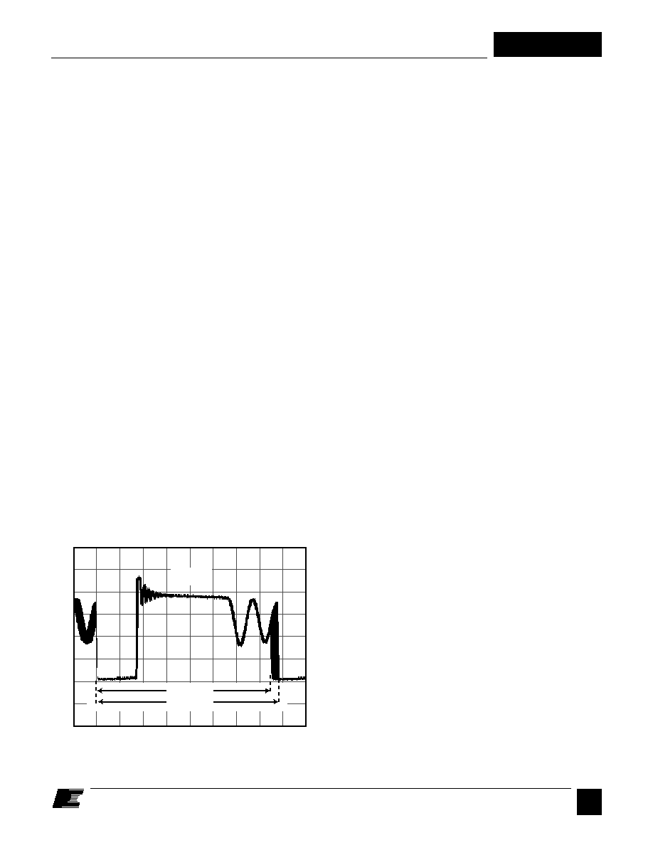
 | –≠–ª–µ–∫—Ç—Ä–æ–Ω–Ω—ã–π –∫–æ–º–ø–æ–Ω–µ–Ω—Ç: TNY256P | –°–∫–∞—á–∞—Ç—å:  PDF PDF  ZIP ZIP |

TNY256
TinySwitch
Plus
Energy Efficient, Low Power Off-line Switcher
August 1999
Æ
Figure 1. Typical Standby Application.
ORDER
PART
NUMBER
85-265
VAC
230 VAC or
115 VAC
w/Doubler
Product Highlights
TinySwitch Plus
Features
∑ Extended power range
∑ Fully integrated auto-restart reduces short circuit current
∑ Line under-voltage sense eliminates turn-off glitches
∑ Frequency jittering dramatically reduces EMI (5 to 10 dB)
∑ TO-220 package option
Lowest Cost, Low Power Switcher Solution
∑ Lower cost than RCC, discrete PWM and other integrated/
hybrid solutions
∑ Cost effective replacement for bulky linear adapters
∑ Lowest component count
∑ Simple ON/OFF control ≠ no loop compensation components
∑ No bias winding ≠ simpler, lower cost transformer
∑ Designed to work with low cost external components
Extremely Energy Efficient
∑ Consumes only 30/60 mW at 115/230 VAC with no load
∑ Meets Blue Angel, Energy Star, Energy 2000 and
200mW European cell phone requirements for standby
∑ Saves $1 to $4 per year in energy costs (at $0.12/kWHr)
compared to bulky linear adapters
∑ Ideal for cellular phone chargers and adapters
High Performance at Low Cost
∑ High voltage powered ≠ ideal for charger applications
∑ High bandwidth provides fast turn on with no overshoot
∑ Current limit operation rejects line frequency ripple
∑ Built-in current limit and thermal protection
Description
The TNY256 extends the power range of the TinySwitch family
of energy efficient, low power off-line switchers. TinySwitch
devices use a breakthrough design to provide the lowest cost,
high efficiency, off-line switching solution for low power
applications. They integrate a 700 V power MOSFET, oscillator,
high voltage switched current source, current limit and thermal
shutdown circuitry into a single, monolithic device. The devices
start-up and operate on power derived from the DRAIN voltage,
eliminating the need for a transformer bias winding and associated
circuitry. TinySwitch's low operating current allows power
supply no-load consumption to be kept under 100 mW, even at
265 VAC input.
TNY256P
OUTPUT POWER CAPABILITY*
PACKAGE
DIP-8
SMD-8
TNY256G
5-10 W
8-15 W
TM
The TinySwitch Plus incorporates auto-restart, line under-voltage
sense, and frequency jittering features. The auto-restart circuit
safely limits output power during fault conditions such as output
short or open loop. The auto-restart circuit is fully integrated and
does not require external timing components. The line under-
voltage sense threshold can be externally programmed using a line
sense resistor. During start-up, this feature keeps the TNY256 off
until the input line voltage reaches the under-voltage threshold.
When the input line voltage is removed, the line under-voltage
circuit prevents auto-restart attempts after the output goes out of
regulation. This eliminates power down glitches caused by the
slow discharge of input storage capacitors present in applications
such as standby supplies. A single resistor is used to implement
this feature, eliminating what normally takes five to six components.
The line sense resistor is optional. The TNY256 operating frequency
of 130 kHz is jittered (frequency modulated) to reduce both quasi-
peak and average EMI, minimizing filtering costs.
Table 1. * The low end of the power ranges shown represent enclosed
adapters with minimal heat sinking whereas, the high end of the power
ranges represent open frame power supplies with adequate heat
sinking, both measured at an ambient of 50
o
C. Please refer to the Key
Application Considerations section for more details.
TNY256Y
TO-220-7B
PI-2363-022699
Wide-Range
HV DC Input
D
S
EN/UV
BP
+
≠
+
≠
DC Output
TinySwitch Plus
Optional
UV Resistor
8-19 W
5-11 W
B
8/99
TNY256
2
Figure 2. Functional Block Diagram.
Figure 3. Pin Configuration.
Pin Functional Description
DRAIN (D) Pin:
Power MOSFET drain connection. Provides internal operating
current for both start-up and steady-state operation.
BYPASS (BP) Pin:
Connection point for a 0.1
µ
F external bypass capacitor for the
internally generated 5.8 V supply.
ENABLE/UNDER-VOLTAGE (EN/UV) Pin:
This pin has dual functions, enable input and line under-voltage
sense. During normal operation, switching of the power
MOSFET is controlled by this pin. MOSFET switching is
terminated when a current greater than 50
µ
A is drawn out of
this pin. This pin also senses line under-voltage conditions
through an external resistor connected to the DC line voltage.
If there is no external resistor connected to this pin, TNY256
detects this and disables the line under-voltage function.
SOURCE (S) Pin:
Power MOSFET source connection. Primary return.
PI-2367-122398
CLOCK
OSCILLATOR
5.8 V
5.1 V
SOURCE
(S)
S
R
Q
DCMAX
BYPASS
(BP)
+
-
VI
LIMIT
LEADING
EDGE
BLANKING
THERMAL
SHUTDOWN
+
-
DRAIN
(D)
REGULATOR
5.8 V
BYPASS PIN
UNDER-VOLTAGE
1.5 V + VTH
ENABLE/
UNDER-VOLTAGE
(EN/UV)
Q
50
µ
A
LINE UNDER-VOLTAGE
RESET
AUTO-
RESTART
COUNTER
JITTER
1.5 V
CLOCK
PI-2500-072199
Tab Internally
Connected to Source Pin
TO-220 (YO7B)
EN/UV
D
S
S
8
5
7
6
1
4
2
3
S
S
S
1 EN/UV
3 BP
5 NC
4 S
7 D
BP
DIP-8 (PO8A)
SMD-8 (GO8A)
NO CONNECT (N) Pin
No connection.
B
8/99
TNY256
3
TinySwitch
Functional Description
TinySwitch combines a high voltage power MOSFET switch
with a power supply controller in one device. Unlike conventional
PWM (Pulse Width Modulator) controllers, TinySwitch uses a
simple ON/OFF control to regulate the output voltage.
The TNY256 controller consists of an Oscillator, Enable (Sense
and Logic) circuit, 5.8 V Regulator, Bypass pin Under-Voltage
circuit, Over Temperature Protection, Current Limit circuit,
Leading Edge Blanking and a 700 V power MOSFET. The
TNY256 incorporates additional circuitry for Line Under-Voltage
Sense, Auto-Restart and Frequency Jitter. Figure 2 shows the
functional block diagram with the most important features.
Oscillator
The typical oscillator frequency is internally set to an average of
130 kHz. Two signals are generated from the oscillator, the
Maximum Duty Cycle signal (DC
MAX
) and the Clock signal that
indicates the beginning of each cycle.
The TNY256 oscillator incorporates circuitry that introduces a
small amount of frequency jitter, typically 5 kHz peak-to-peak,
to minimize EMI emission. The modulation rate of the frequency
jitter (1 kHz) is set to optimize EMI reduction for both average
and quasi-peak emissions. The frequency jitter should be
measured with the oscilloscope triggered at the falling edge of
the DRAIN waveform. The waveform in Figure4 illustrates the
frequency jitter of the TNY256.
Enable Input Circuit
The enable input circuit at the EN/UV pin consists of a low
impedance source follower output set at 1.5 V. The current
through the source follower is limited to 50
µ
A with 10
µ
A of
hysteresis. When the current drawn out of the this pin exceeds
50
µ
A, a low logic level (disable) is generated at the output of
the enable circuit. This output is sampled at the beginning of
each cycle on the rising edge of the clock signal. If high, the
power MOSFET is turned on for that cycle (enabled), otherwise
the power MOSFET remains off (disabled). Since the sampling
is done only at the beginning of each cycle, subsequent
changes in the EN/UV pin voltage or current during the
remainder of the cycle are ignored.
Under most operating conditions (except when close to no-
load), the low impedance of the source follower, keeps the
voltage on the EN/UV pin from going much below 1.5 V, in the
disabled state. This improves the response time of the
optocoupler that is usually connected to this pin.
5.8 V Regulator
The 5.8 V regulator charges the bypass capacitor connected to
the BYPASS pin to 5.8 V by drawing a current from the voltage
on the DRAIN, whenever the MOSFET is off. The BYPASS
pin is the internal supply voltage node for the TinySwitch.
When the MOSFET is on, the TinySwitch runs off of the energy
stored in the bypass capacitor. Extremely low power
consumption of the internal circuitry allows the TinySwitch to
operate continuously from the current drawn from the DRAIN
pin. A bypass capacitor value of 0.1
µ
F is sufficient for both
high frequency de-coupling and energy storage.
BYPASS Pin Under-Voltage
The BYPASS pin under-voltage circuitry disables the power
MOSFET when the BYPASS pin voltage drops below 5.1 V.
Once the BYPASS pin voltage drops below 5.1 V, it must rise
back to 5.8 V to enable (turn-on) the power MOSFET.
Over Temperature Protection
The thermal shutdown circuitry senses the die temperature.
The threshold is set at 135
o
C with 70
o
C hysteresis. When the
die temperature rises above this threshold (135
o
C) the power
MOSFET is disabled and remains disabled until the die
temperature falls by 70
o
C, at which point it is re-enabled.
Current Limit
The current limit circuit senses the current in the power
MOSFET. When this current exceeds the internal threshold
(I
LIMIT
), the power MOSFET is turned off for the remainder of
that cycle.
The leading edge blanking circuit inhibits the current limit
comparator for a short time (t
LEB
) after the power MOSFET is
turned on. This leading edge blanking time has been set so that
current spikes caused by primary-side capacitance and
secondary-side rectifier reverse recovery time will not cause
premature termination of the switching pulse.
Auto-Restart
In the event of a fault condition such as output overload, output
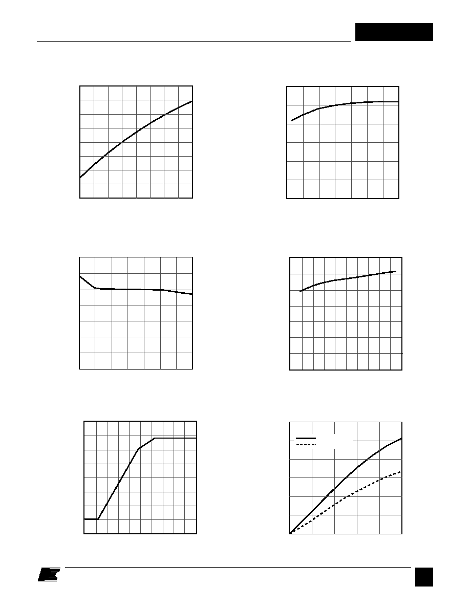
Figure 4. Frequency Jitter.
PI-2366-021299
0
.5
1
Time (
µ
s)
0
100
200
400
500
600
300
V
DRAIN
132.5 kHz
127.5 kHz
B
8/99
TNY256
4
short, or an open loop condition, TNY256 enters into auto-
restart operation. An internal counter clocked by the oscillator
gets reset every time the EN/UV pin is pulled low. If the EN/
UV pin is not pulled low for 32 ms, the power MOSFET
switching is disabled for 128 ms (except in the case of line
under-voltage condition). The auto-restart alternately enables
and disables the switching of the power MOSFET until the fault
condition is removed. Figure 5 illustrates auto-restart circuit
operation in the presence of a temporary output short.
In the event of line under-voltage condition, the switching of the
power MOSFET is disabled beyond its normal 128 ms time
until the line under-voltage condition goes away.
Line Under-Voltage (UVLO) Sense Circuit
The DC line voltage can be monitored by connecting an
external resistor from the DC line to the EN/UV pin. During
power-up or when the switching of the power MOSFET is
disabled in auto-restart, the current into the EN/UV pin must
exceed 50
µ
A to initiate switching of the power MOSFET.
During power-up, this is implemented by holding the BYPASS
pin to 5.1 V while the line under-voltage condition exists. The
BYPASS pin then rises from 5.1 V to 5.8V when the line under-
voltage condition goes away. When the switching of the power
MOSFET is disabled in auto-restart mode and the line under-
voltage condition exists, the counter is stopped. This stretches
the disable time beyond its normal 128ms until the line under-
voltage condition goes away.
The line under-voltage circuit also detects when there is no
external resistor connected to the EN/UV pin. In this case the
line under-voltage function is disabled.
TinySwitch
Operation
TinySwitch devices operate in the current limit mode. When
enabled, the oscillator turns the power MOSFET on at the
beginning of each cycle. The MOSFET is turned off when the
current ramps up to the current limit. The maximum on-time of
the MOSFET is limited to DC
MAX
by the oscillator. Since the
current limit and frequency of the TNY256 is constant, the
power delivered is proportional to the primary inductance of the
transformer and is relatively independent of the input voltage.
Therefore, the design of the power supply involves calculating
the primary inductance of the transformer for the maximum
power required. If the TNY256 is appropriately chosen for the
PI-2377-120998
V
DRAIN
V
EN
CLOCK
D
DRAIN
I
MAX
Figure 5. TNY256 Auto-Restart Operation.
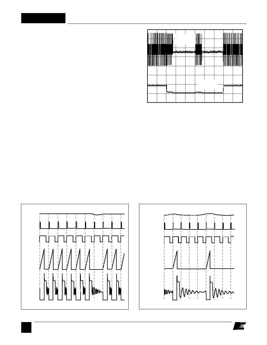
Figure 6. TNY256 Operation at Heavy Load.
Figure 7. TNY256 Operation at Light Load.
V
DRAIN
V
EN
CLOCK
D
DRAIN
I
MAX
PI-2373-120998
PI-2342-121198
0
250
500
Time (ms)
0
10
0
20
100
200
300
DRAIN
VOLTAGE
OUTPUT
VOLTAGE
B
8/99
TNY256
5
power level at the lowest input voltage, the calculated inductance
will ramp up the current to the current limit before the DC
MAX
limit is reached.
Enable Function
TNY256 senses the EN/UV pin to determine whether or not to
proceed with the next switch cycle as described earlier. Once
a cycle is started, it always completes the cycle (even when the
EN/UV pin changes state half way through the cycle). This
operation results in a power supply whose output voltage ripple
is determined by the output capacitor, amount of energy per
switch cycle and the delay of the feedback.
The EN/UV pin signal is generated on the secondary by
comparing the power supply output voltage with a reference
voltage. The EN/UV pin signal is high when the power supply
output voltage is less than the reference voltage.
In a typical implementation, the EN/UV pin is driven by an
optocoupler. The collector of the optocoupler transistor is
connected to the EN/UV pin and the emitter is connected to the
SOURCE pin. The optocoupler LED is connected in series with
a Zener across the DC output voltage to be regulated. When the
output voltage exceeds the target regulation voltage level
(optocoupler diode voltage drop plus Zener voltage), the
optocoupler diode will start to conduct, pulling the EN/UV pin
low. The Zener can be replaced by a TL431 device for
improved accuracy.
The EN/UV pin pull-down current threshold is nominally
50
µ
A, but is set to 40
µ
A the instant the threshold is exceeded.
This is reset back to 50
µ
A when the EN/UV pull-down current
drops below the current threshold of 40
µ
A.
ON/OFF Control
The internal clock of the TNY256 runs all the time. At the
beginning of each clock cycle, it samples the EN/UV pin to
decide whether or not to implement a switch cycle. If the EN/
UV pin is high (< 40
µ
A), then a switching cycle takes place. If
the EN/UV pin is low (greater than 50
µ
A) then no switching
cycle occurs, and the EN/UV pin status is sampled again at the
start of the subsequent clock cycle.
At full load, TNY256 will conduct during the majority of its
clock cycles (Figure6). At loads less than full load, it will
"skip" more cycles in order to maintain voltage regulation at the
secondary output. At light load or no load, almost all cycles will
be skipped (Figure7). A small percentage of cycles will
conduct to support the power consumption of the power supply.
The response time of the TNY256 ON/OFF control scheme is
very fast compared to normal PWM control. This provides tight
regulation and excellent transient response.
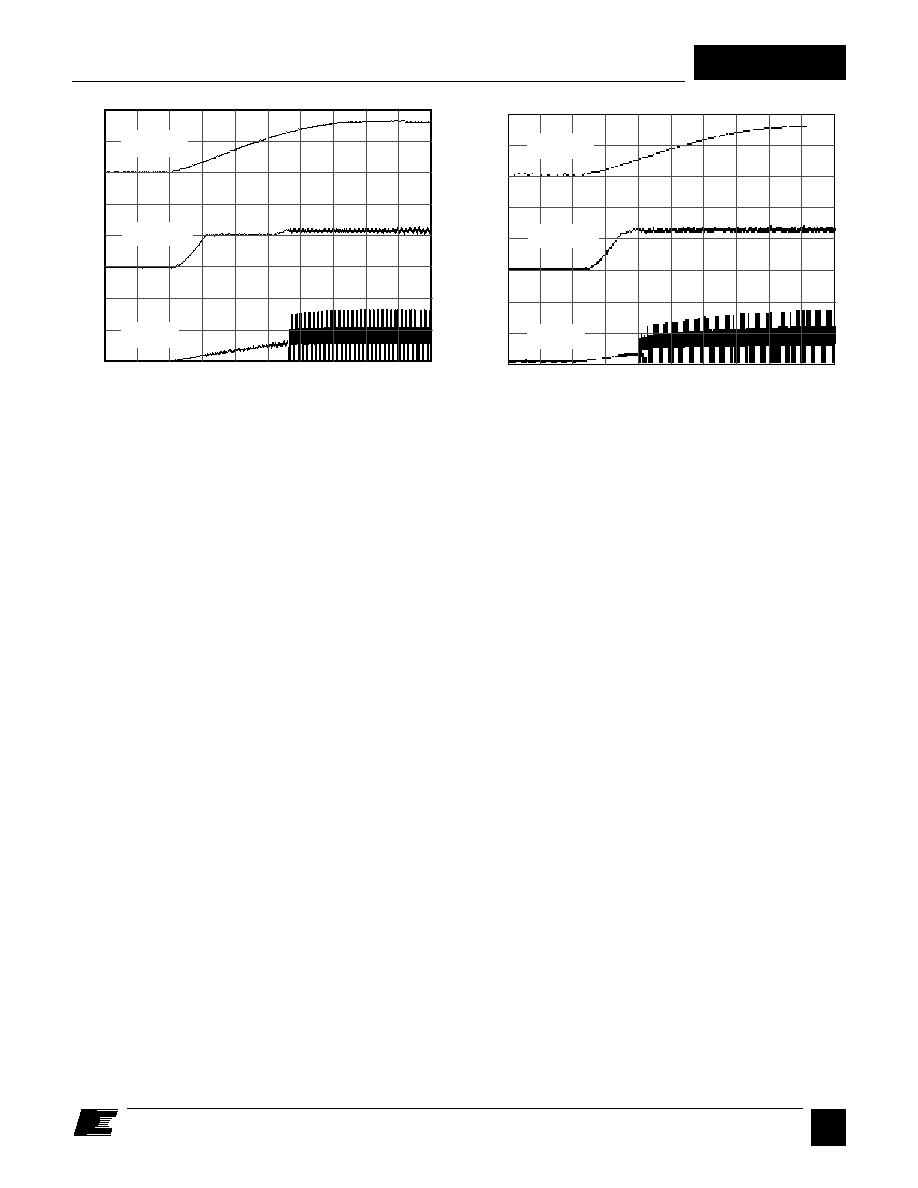
Power Up/Down
The TNY256 requires only a 0.1
µ
F capacitor on the BYPASS
pin. Because of the small size of this capacitor, the power-up
delay is kept to an absolute minimum, typically 0.3 ms. Due to
the fast nature of the ON/OFF feedback, there is no overshoot
at the power supply output. When an external resistor (2 M
)
is connected to the EN/UV pin, the power MOSFET switching
will be delayed during power-up until the DC line voltage
exceeds the threshold (100 V). Figures 8 and 9 illustrate the
power-up timing waveform of TNY256 in applications with
and without an external resistor (2 M
) connected to the
EN/UV pin.
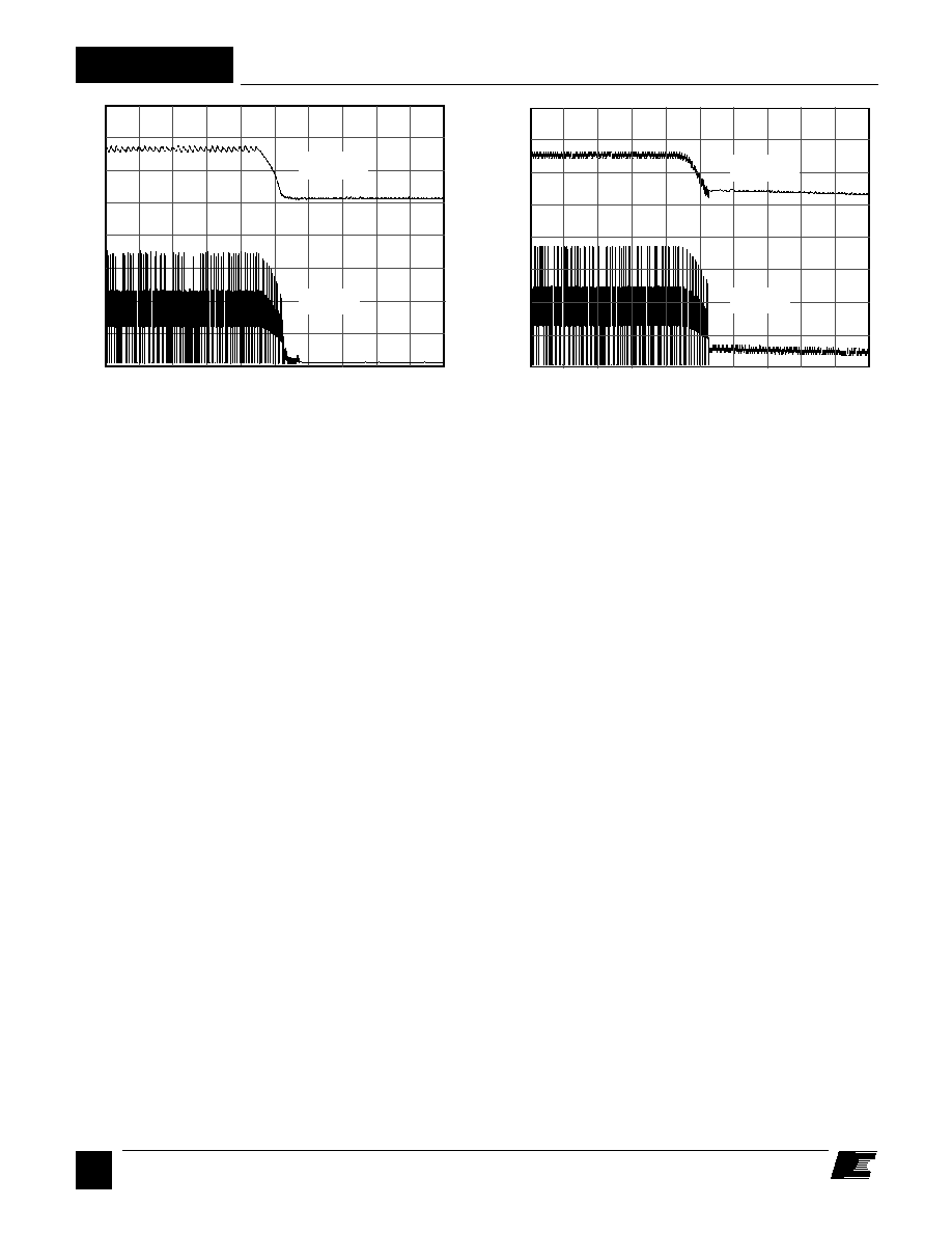
During power-down, when an external resistor is used, the
Figure 8. TNY256 Power-up With External Resistor (2 M
)
Connected to EN/UV Pin.
Figure 9. TNY256 Power-up Without External Resistor Connected
to EN/UV Pin.
PI-2381-122398
0
1
2
Time (ms)
0
200
400
5
0
10
0
100
200
V
DC-BUS
V
BYPASS
V
DRAIN
0
1
2
Time (ms)
0
200
400
5
0
10
0
100
200
PI-2383-122398
V
DC-BUS
V
BYPASS
V
DRAIN
B
8/99
TNY256
6
Figure 10. Normal Power-down Timing.
Figure 11. Slow Power-down Timing with External (2 M
)
Resistor Connected to EN/UV Pin.
PI-2348-010599
0
.5
1
Time (s)
0
100
200
300
0
100
200
400
V
DC-BUS
V
DRAIN
PI-2395-010599
0
2.5
5
Time (s)
0
100
200
400
300
0
100
200
V
DC-BUS
V
DRAIN
power MOSFET will switch for 32 ms after the output loses
regulation. The power MOSFET will then remain off without
any glitches since the under-voltage function prohibits restarts
when the line voltage is low.
Figure 10 illustrates a typical power-down timing waveform of
TNY256. Figure 11 illustrates a very slow power-down timing
waveform of TNY256 as in standby applications. The external
resistor (2 M
) is connected to the EN/UV pin in this case to
prevent restarts.
The TNY256 does not require a bias winding to provide power
to the chip, because it draws the power directly from the DRAIN
pin (see Functional Description above). This has two main
benefits. First, for a nominal application, this eliminates the
cost of an extra bias winding and associated components.
Secondly, for charger applications, the current-voltage
characteristic often allows the output voltage to fall to low
values while still delivering power. This type of application
normally requires a forward-bias winding which has many
more associated components, none of which are necessary with
the TNY256.
Current Limit Operation
Each switching cycle is terminated when the DRAIN current
reaches the current limit of the TNY256. For a given primary
inductance and input voltage, the duty cycle is constant.
However, the duty cycle does change inversely with the input
voltage providing "voltage feed-forward" advantages: good
line ripple rejection and relatively constant power delivery
independent of the input voltage.
BYPASS Pin Capacitor
The BYPASS pin uses a small 0.1
µ
F ceramic capacitor for
decoupling the internal power supply of the TNY256.
Application Example
The TNY256 is ideal for low cost, high efficiency power
supplies in a wide range of applications such as PC standby,
cellular phone chargers, AC adapters, motor control, appliance
control and ISDN network termination. The 130 kHz operation
allows the use of a low cost EE16 core transformer while still
providing good efficiency. The frequency jitter in TNY256
makes it possible to use a single inductor (or two small resistors
if lower efficiency is acceptable) in conjunction with two input
capacitors for input EMI filtering up to the 10W level. The
auto-restart function allows the design to be optimized for
maximum efficiency without consideration for short-circuit
current on the secondary. For applications requiring under-
voltage lockout (UVLO), the TNY256 eliminates several
components and saves cost.
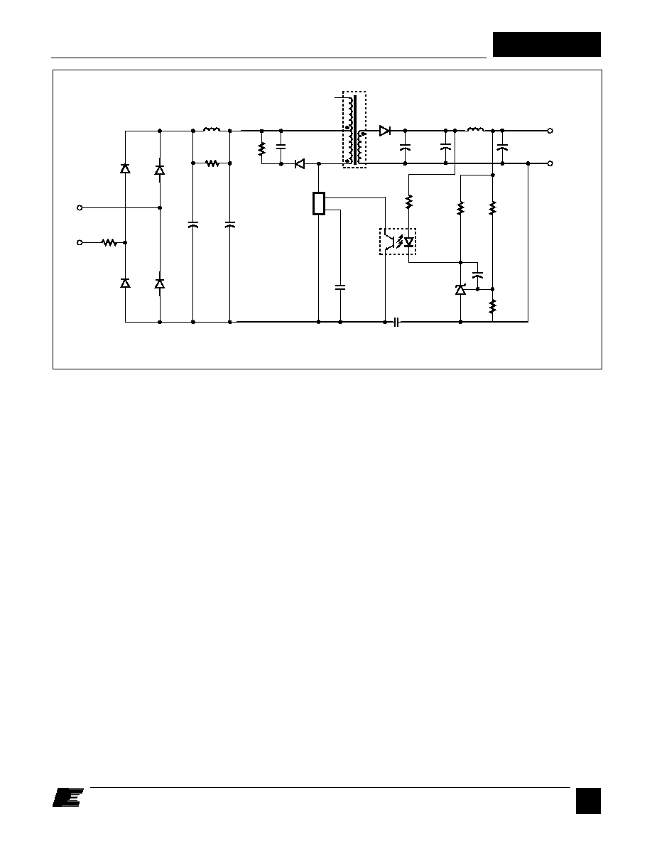
As an example, Figure12 shows a 9 V, 0.6 A, AC adapter
operating from a universal input range (85-265 VAC). The AC
input is rectified and filtered by D1-D4, C1 and C2 to create a
high voltage DC bus which is connected to T1. Inductor L1
forms a pi-filter in conjunction with C1 and C2. The resistor R1
damps resonance in inductor L1. The frequency jitter in
TNY256 allows it to meet worldwide conducted EMI standards
using a simple pi-filter in combination with a small value
Y1-capacitor C5 and a shield winding between primary and
secondary windings inside transformer T1. Diode D5, capacitor
C3 and resistor R3 form an RCD clamp circuit that limits the
turn-off voltage spike to a safe value on the TNY256 DRAIN
pin.
The secondary winding is rectified and filtered by D6, C6 and
C7 to provide the 9 V output. Additional filtering is provided
by L3 and C8. The output voltage is determined by the resistor
network R7 and R8. Resistor R9 maintains a bias current
B
8/99
TNY256
7
Figure 12. 5.5 W AC Adaptor with Universal Input (85-265 VAC).
through the TL431 voltage reference for proper regulation.
Capacitor C11 bypasses the TL431 response for improved
ripple performance. Resistor R5 determines the AC gain of the
circuit.
Key Application Considerations
For the most up to date information visit our website
at:
www.powerint.com
Design
Output Power
Table 1 shows the practical maximum continuous output power
levels obtainable under following conditions:
1. The minimum DC input voltage is 90 V or higher for 85 VAC
input or 240 V or higher for 230VAC input or 115 VAC
input with a voltage doubler. This corresponds to a filter
capacitor of 3
µ
F/W for universal input and 1
µ
F/W for 230
or 115 VAC w/doubler input.
2. A secondary output of 5 V with a Schottky rectifier diode.
3. The P and G packaged parts are board mounted with source
pins soldered to sufficient area of copper and the Y packaged
parts are heat sinked sufficiently to keep the die temperature
at or below 100
o
C.
The maximum power capability of TinySwitch in a given
application depends on the thermal environment (sealed
enclosure, ventilated, open frame, etc.,), transformer core size
and design (continuous or discontinuous), efficiency required,
minimum specified input voltage, input storage capacitance,
output voltage, output diode forward drop, etc., and can be
different from the values shown in Table 1.
Audible Noise
At loads other than maximum load, the cycle skipping mode
operation used in TinySwitch can generate audio frequency
components in the transformer. This can cause the transformer
to produce audio noise. Transformer audible noise can be
reduced by using appropriate transformer construction
techniques and decreasing the peak flux density. For more
information on audio suppression techniques, please check the
Application Notes section on our web site at www.powerint.com.
Ceramic capacitors that use dielectrics such as Z5U, when used
in clamp and snubber circuits, can also generate audio noise due
to electrostriction and piezo-electric effects. If this is the case,
replacing them with a capacitor having a different type of
dielectric is the simplest solution. Polyester film capacitors and
ceramic capacitors with dielectrics such as NPO or X7R are
good alternatives.
PI-2502-072699
TinySwitch Plus
D
S
EN/UV
BP
+ 9 V
0.6 A
RTN
D1
1N4005
C1
10
µ
F
400 V
Fusible
RF1
10
C4
0.1
µ
F
85-265
VAC
L1
470
µ
H
D2
1N4005
D3
1N4005
D4
1N4005
R3
330 K
1/4 W
U2
SFH615-2
D6
MBR360
L3
18
µ
H
C6
330
µ
F
16 V
C2
10
µ
F
400 V
C8
220
µ
F
10 V
R5
100
R9
470
U3
TL431CLP
C5
2200 pF
Y1 Safety
U1
TNY256P
C3
10 nF
D5
1N4937
T1
R1
4.7 K
1
4
8
10
R7
26.1 K
R8
10 K
C11
0.1
µ
F
C7
330
µ
F
16 V
2
NC

B
8/99
TNY256
8
Figure 13. Recommended PC Layout for TinySwitch without Under-Voltage Lock Out Resister.
Layout
Single Point Grounding
Use a single point ground connection at the SOURCE pin for the
BYPASS pin capacitor and the Input Filter Capacitor (see
Figure 13).
Primary Loop Area
The area of the primary loop that connects the input filter
capacitor, transformer primary and TinySwitch together, should
be kept as small as possible.
Primary Clamp Circuit
A clamp or snubber circuit is used to minimize peak voltage and
ringing on the DRAIN pin at turn-off. This can be achieved by
using an RC snubber for less than 3 W or an RCD clamp as
shown in Figure 13 for higher power. A Zener and diode clamp
across the primary or a single 550V Zener clamp from DRAIN
to SOURCE can also be used. In all cases care should be taken
to minimize the circuit path from the snubber/clamp components
to the transformer and TinySwitch.
Thermal Considerations
Copper underneath the TinySwitch acts not only as a single point
ground, but also as a heatsink. The hatched area shown in
Figure13 should be maximized for good heat-sinking of
TinySwitch and output diode.
EN/UV pin layout optimization
The EN/UV pin connection to the opto-coupler should be kept
to an absolute minimum (less than 0.5 in.), and this connection
should be kept away from the DRAIN pin (minimum of 0.2 in.).
These distance limitations are critical only in applications
where an external under-voltage resistor (2 M
) is not used.
Y-Capacitor
The placement of the Y-capacitor should be directly from the
primary single point ground to the common/return terminal on
the secondary side. Such placement will maximize the EMI
benefit of the Y-capacitor.
Optocoupler
It is important to maintain the minimum circuit path from the
optocoupler transistor to the TinySwitch EN/UV and SOURCE
pins to minimize noise coupling.
Output Diode
For best performance, the area of the loop connecting the
secondary winding, the Output Diode and the Output Filter
Capacitor, should be minimized. See Figure13 for optimized
layout. In addition, sufficient copper area should be provided
at the anode and cathode terminals of the diode to adequately
heatsink the diode under output short circuit conditions.
Input and Output Filter Capacitors
There are constrictions in the traces connected to the input and
output filter capacitors. These constrictions are present for two
reasons. The first is to force all the high frequency currents to
flow through the capacitor (if the trace were wide then it could
flow around the capacitor). Secondly, the constrictions minimize
the heat transferred from the TinySwitch to the input filter
capacitor and from the secondary diode to the output filter
capacitor. The common/return (the negative output terminal in
Figure13) terminal of the output filter capacitor should be
connected with a short, low resistance path to the secondary
winding. In addition, the common/return output connection
should be taken directly from the secondary winding pin and not
from the Y-capacitor connection point.
TOP VIEW
PI-2360-012199
Y1-
Capacitor
Opto-
coupler
C
BP
D
EN/UV
BP
TinySwitch
+
≠
HV
+
≠
DC
Out
Input Filter Capacitor
Output Filter Capacitor
Safety Spacing
Transformer
Maximize hatched copper
areas ( ) for optimum
heat sinking
S
S
PRI
SEC
B
8/99
TNY256
9
BYPASS Voltage .......................................... -0.3 V to 9 V
Storage Temperature ..................................... -65 to 125
∞
C
Operating Junction Temperature
(2)
................ -40 to 150
∞
C
Lead Temperature
(3)
................................................ 260
∞
C
3. 1/16" from case for 5 seconds.
ABSOLUTE MAXIMUM RATINGS
(1)
DRAIN Voltage ....................................... - 0.3 V to 700 V
Peak DRAIN Current ............................................. 800 mA
EN/UV Voltage ............................................ - 0.3 V to 9 V
EN/UV Current ...................................................... 100 mA
1. All voltages referenced to SOURCE, T
A
= 25
∞
C.
2. Normally limited by internal circuitry.
S1 Open
See Note 1
I
EN/UV
= -25
µ
A
I
EN/UV
= 25
µ
A
V
EN/UV
= 0 V
(MOSFET Not Switching)
See Note 2
-68
-50
-28
-15
-10
-5
1.10
1.45
1.80
-58
-35
215
CONTROL FUNCTIONS
Output
Frequency
Maximum
Duty Cycle
EN/UV Pin Turnoff
Threshold Current
EN/UV Pin
Hysteresis Current
EN/UV Pin
Voltage
EN/UV Short-
Circuit Current
DRAIN
Supply Current
BYPASS Pin
Charge Current
kHz
%
µ
A
µ
A
V
µ
A
µ
A
µ
A
mA
mA
Min
Typ
Max
f
OSC
DC
MAX
I
DIS
I
HYS
V
EN
I
ENSC
I
S1
I
S2
I
CH1
I
CH2
Parameter
Symbol
(Unless Otherwise Specified)
See Figure 14
Conditions
130
255
-5.50
-4.10
EN/UV Open
(MOSFET Switching)
See Note 2, 3
T
j
= 25
∞
C
See Figure 4
Units
SOURCE = 0 V
;
T
j
= -40 to 125
∞
C
66
T
j
= -40
∞
C to 125
∞
C
T
j
= 125
∞
C
-52
V
EN/UV
= 0 V, T
j
= -40
∞
C to 125
∞
C
V
EN/UV
= 0 V, T
j
= 125
∞
C
-45
V
BP
= 0 V, T
j
= 25
∞
C
See Note 4,5
V
BP
= 4 V, T
j
= 25
∞
C
See Note 4,5
170
2.70
-40
5.0
Average
Peak-Peak Jitter
115
140
63
69
3.8
6.2
-68
-41
1.85
3.25
-58
-25
300
-3.75
-7.50
-6.00
-2.25
Thermal Impedance: Y Package (
JA
)
(1)
............... 70
∞
C/W
(
JC
)
(2)
................. 2
∞
C/W
P/G Package:
(
JA
) ........ 45
∞
C/W
(3)
; 35
∞
C/W
(4)
(
JC
)
(2)
............................ 5
∞
C/W
1. Free standing with no heatsink.
2. Measured at tab closest to plastic interface or source pin.
3. Soldered to 0.36 sq. inch (232mm
2
), 2oz (610 gm/m
2
) copper
clad.
4. Soldered to 1 sq. inch (645mm
2
), 2oz. (610 gm/m
2
) copper clad
THERMAL IMPEDANCE
B
8/99
TNY256
10
See Note 4
T
j
= 25
∞
C
See Figure 17
T
j
= 25
∞
C
Conditions
Parameter
Symbol
SOURCE = 0 V; T
j
= -40 to 125
∞
C
See Figure 14
(Unless Otherwise Specified)
V
BP
V
BPH
I
LUV
I
LIMIT
I
INIT
t
LEB
t
ILD
R
DS(ON)
I
DSS
BV
DSS
t
r
t
f
mA
mA
ns
ns
∞
C
∞
C
µ
A
V
ns
ns
BYPASS Pin
Voltage
BYPASS
Hysteresis
EN/UV Pin Line
Under-voltage
Threshold
Current Limit
Initial Current
Limit
Leading Edge
Blanking Time
Current Limit
Delay
Thermal Shutdown
Temperature
Thermal Shutdown
Hysteresis
ON-State
Resistance
OFF-State
Leakage
Breakdown
Voltage
Rise Time
Fall Time
Min
Typ
Max
Units
CONTROL FUNCTIONS (cont.)
V
BP
= 6.2 V, V
EN/UV
= 0 V,
V
DS
= 560 V, T
j
= 125
∞
C
T
j
= 25
∞
C
T
j
= 100
∞
C
Measured in a Typical Flyback
Converter Application.
V
BP
= 6.2 V, V
EN/UV
= 0 V,
I
DS
= 100
µ
A, T
j
= 25
∞
C
T
j
= 25
∞
C
See Note 8, 9
I
D
= 50 mA
5.85
V
6.10
T
j
= 25
∞
C
See Note 8
0.72
0.85
0.60
V
di/dt = 120 mA/
µ
s, T
j
= 25
∞
C
See Note 7
5.60
50
55
44
µ
A
CIRCUIT PROTECTION
450
500
550
0.65 x
l
LIMIT(MIN)
170
215
100
150
125
135
145
70
15.6
18.0
25.7
30.0
50
700
50
50
OUTPUT

B
8/99
TNY256
11
NOTES:
1. For a threshold with a negative value, negative hysteresis is a decrease in magnitude of the corresponding threshold.
2. Total current consumption is the sum of I
S1
and I
DSS
when EN/UV pin is shorted to ground (MOSFET not switching)
and the sum of I
S2
and I
DSS
when EN/UV pin is open (MOSFET switching).
3. Since the output MOSFET is switching, it is difficult to isolate the switching current from the supply current at the
DRAIN. An alternative is to measure the BYPASS pin current at 6.2 V.
4. BYPASS pin is not intended for sourcing supply current to external circuitry.
5. See typical performance characteristics section for BYPASS pin start-up charging waveform.
6. For current limit at other di/dt values, refer to current limit vs. di/dt curve under typical performance
characteristics.
7. This parameter is derived from characterization.
8. This parameter is derived from the change in current limit measured at 5X and 10X of the di/dt shown in the I
LIMIT
specification.
9. Auto-restart on time has the same temperature characteristics as the oscillator (inversely proportional to
frequency).
Conditions
Parameter
Symbol
SOURCE = 0 V; T
j
= -40 to 125
∞
C
See Figure 14
(Unless Otherwise Specified)
50
0.5
t
EN/UV
t
DST
V
µ
s
µ
s
ms
%
DRAIN Supply
Voltage
Output EN/UV
Delay
Output Disable
Setup Time
Min
Typ
Max
Units
OUTPUT (cont.)
10
Auto-Restart,
ON-Time
Auto-Restart
Duty Cycle
t
AR
DC
AR
32.0
20
28.9
35.2
T
j
= 25
∞
C
See Note 10
24
16
See Note 8

B
8/99
TNY256
12
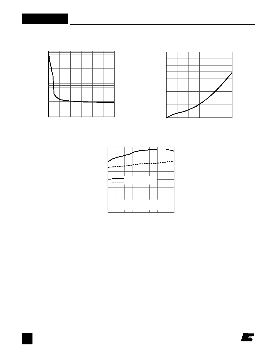
Figure 17. Current Limit Envelope.
Figure 15. TinySwitch Duty Cycle Measurement.
Figure 16. TinySwitch Output Enable Timing.
PI-2048-050798
DRAIN
VOLTAGE
HV
0 V
90%
10%
90%
t2
t1
D =
t1
t2
Figure 14. TinySwitch General Test Circuit.
PI-2352-011899
0.1
µ
F
10 V
50 V
470
5 W
S2
470
NOTE: This test circuit is not applicable for current limit or output characteristic measurements.
D EN/UV
BP
S
S
S
S
S
150 V
S1
2 M
PI-2364-012699
EN/UV
tP
tEN/UV
DC
MAX
t
P
=
1
f
OSC
V
DRAIN
(internal signal)
0.8
1.3
1.2
1.1
0.9
0.8
1.0
0
0
1
2
6
8
3
Time (
µ
s)
DRAIN Current (normalized)
PI-2362-012699
4
5
7
0.7
0.6
0.5
0.4
0.3
0.2
0.1
ILIMIT(MAX) @ 25 ∞C
ILIMIT(MIN) @ 25 ∞C
IINIT(MIN)
tLEB (Blanking Time)
B
8/99
TNY256
13
Typical Performance Characteristics
1.1
1.0
0.9
-50 -25
0
25
50
75 100 125 150
Junction Temperature (
∞
C)
Breakdown Voltage (V)
(Normalized to 25
∞
C)
BREAKDOWN vs. TEMPERATURE
PI-2213-051198
1.2
1.0
0.8
0.6
0.4
0.2
0
-50
-25
0
25
50
75
100 125
Junction Temperature (
∞
C)
FREQUENCY vs. TEMPERATURE
PI-2356-011899
Output Frequency
1.2
1.0
0.8
0.6
0.4
0.2
0.0
0
240
480
720
960
1200
di/dt in mA/
µ
s
CURRENT LIMIT vs. di/dt
PI-2234-082798
Current Limit
(Normalized to 120 mA/
µ
s)
1.4
1.2
1.0
0.8
0.6
0.4
0.2
0.0
-50
-25
0
25
50
75
100 125
Temperature (
∞
C)
CURRENT LIMIT vs. TEMPERATURE
PI-2354-011899
1.4
Current Limit (A)
(Normalized to 25
∞
C)
6
5
4
3
2
1
0
0
0.2
0.4
0.6
0.8
1.0
Time (ms)
BYPASS PIN START-UP WAVEFORM
PI-2240-082898
BYPASS Pin Voltage (V)
7
DRAIN Voltage (V)
Drain Current (mA)
OUTPUT CHARACTERISTIC
600
500
400
200
100
300
0
0
2
4
6
8
10
T
CASE
=25
∞
C
T
CASE
=100
∞
C
PI-2385-121798
B
8/99
TNY256
14
80
40
0
-40 -20
0
20
40
60
80 100 110
Temperature (
∞
C)
Input Voltage (VAC)
UNDERVOLTAGE THRESHOLD
PI-2358-012099
* 2 M
resistor connected to EN/UV pin.
** Load dependant and determined by the level
of the device upon entering auto-restart.
Power-up*
Power-down at 8 W**
100
1
0
600
DRAIN Voltage (V)
DRAIN Capacitance (pF)
COSS vs. DRAIN VOLTAGE
10
PI-2387-121798
200
400
100
60
80
20
40
0
0
200
400
600
DRAIN Voltage (V)
Power (mW)
DRAIN CAPACITANCE POWER
PI-2389-121798
Typical Performance Characteristics (cont.)

B
8/99
TNY256
15
Notes

B
8/99
TNY256
16
Notes

B
8/99
TNY256
17
Notes
B
8/99
TNY256
18
PI-2076-031197
1
A
K
J1
4
L
G
8
5
C
N
P08A
Plastic DIP-8
D S .004 (.10)
J2
-E-
-D-
B
-F-
DIM
A
B
C
G
H
J1
J2
K
L
M
N
P
Q
inches
0.370-0.385
0.245-0.255
0.125-0.135
0.015-0.040
0.120-0.135
0.060 (NOM)
0.014-0.022
0.010-0.012
0.090-0.110
0.030 (MIN)
0.300-0.320
0.300-0.390
0.300 BSC
mm
9.40-9.78
6.22-6.48
3.18-3.43
0.38-1.02
3.05-3.43
1.52 (NOM)
0.36-0.56
0.25-0.30
2.29-2.79
0.76 (MIN)
7.62-8.13
7.62-9.91
7.62 BSC
Notes:
1. Package dimensions conform to JEDEC
specification MS-001-AB for standard dual
in-line (DIP) package .300 inch row spacing
(PLASTIC) 8 leads (issue B, 7/85)..
2. Controlling dimensions are inches.
3. Dimensions shown do not include mold
flash or other protrusions. Mold flash or
protrusions shall not exceed .006 (.15) on
any side.
4. D, E and F are reference datums on the
molded body.
H
M
P
Q
PI-2077-050798
1
A
J1
4
L
8
5
C
G08A
Plastic SMD-8
D S .004 (.10)
J2
E S .010 (.25)
-E-
-D-
B
-F-
M
J3
DIM
A
B
C
G
H
J1
J2
J3
J4
K
L
M
P
inches
0.370-0.385
0.245-0.255
0.125-0.135
0.004-0.012
0.036-0.044
0.060 (NOM)
0.048-0.053
0.032-0.037
0.007-0.011
0.010-0.012
0.100 BSC
0.030 (MIN)
0.372-0.388
0-8∞
mm
9.40-9.78
6.22-6.48
3.18-3.43
0.10-0.30
0.91-1.12
1.52 (NOM)
1.22-1.35
0.81-0.94
0.18-0.28
0.25-0.30
2.54 BSC
0.76 (MIN)
9.45-9.86
0-8∞
Notes:
1. Package dimensions conform to JEDEC
specification MS-001-AB (issue B, 7/85)
except for lead shape and size.
2. Controlling dimensions are inches.
3. Dimensions shown do not include mold
flash or other protrusions. Mold flash or
protrusions shall not exceed .006 (.15) on
any side.
4. D, E and F are reference datums on the
molded body.
K
G
H
.004 (.10)
J4
P
.010 (.25) M A S
B
8/99
TNY256
19
PIN 1 & 7
B
K
F (Note 7)
G
N
L
M
J
A
O
DIM
A
B
D
E
F
G
H
J
K
L
M
N
O
P
Q
R
S
T
A1
A2
A3
A4
A5
A6
A7
A8
PI-2374-040799
inches
.467-.487
.400-.415
.146 - .156
.108 REF.
.026-.032
.050 BSC
.150 BSC
.860-.880
.045-.055
.095-.115
.015-.020
.165-.185
.236-.260
.570 REF.
.670 REF.
.190-.210
.040-.060
.040-.060
.050
.050
.150
.150
.050
.050
.200
.180 REF.
mm
11.86-12.37
10.16-10.54
3.71-3.96
2.74 REF.
.66-.81
1.27 BSC
3.81 BSC
21.84-22.35
1.14-1.40
2.41-2.92
.38-.51
4.19-4.70
5.99-6.60
14.48 REF.
17.02 REF.
4.83-5.33
1.02-1.52
1.02-1.52
1.27
1.27
3.81
3.81
1.27
1.27
5.08
4.58 REF.
H
D
E
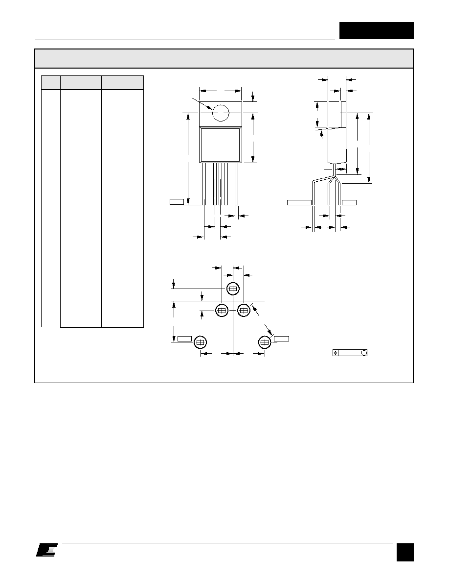
Notes:
1. Controlling dimensions are
inches.
2. Pin numbers start with Pin 1, and
continue from left to right when
viewed from the top.
3. Dimensions shown do not include
mold flash or other protrusions. Mold
flash or protrusions shall not exceed
.006 (.15 mm) on any side.
4. Position of terminals to be
measured at a position .25 (6.35 mm)
below the package body.
5. All terminals are solder plated.
6. Pins 2 and 6 omitted.
7.
Y07B
Plastic TO-220-7B
7∞ TYP.
P
Q
R
S
T
PIN 1
PIN 4
+
PIN 1
PIN 7
MOUNTING HOLE PATTERN
A1
A5
A7
A6
A3
A4
A8
A2
.010 (.25) M

B
8/99
TNY256
20
Notes
-
1) TO-220-7B package information added.
2) I
LUV
minimum increased to 44
µ
to reflect production improvements.
Date
3/99
8/99
Revision
A
B
KOREA
Power Integrations International
Holdings, Inc.
Rm# 402, Handuk Building,
649-4 Yeoksam-Dong, Kangnam-Gu,
Seoul, Korea
Phone:
+82∑2∑568∑7520
Fax:
+82∑2∑568∑7474
JAPAN
Power Integrations, K.K.
Keihin-Tatemono 1st Bldg.
12-20 Shin-Yokohama 2-Chome,
Kohoku-ku, Yokohama-shi,
Kanagawa 222, Japan
Phone:
+81∑45∑471∑1021
Fax:
+81∑45∑471∑3717
EUROPE & AFRICA
Power Integrations (Europe) Ltd.
Centennial Court
Easthampstead Road
Bracknell
Berkshire RG12 1YQ,
United Kingdom
Phone:
+44∑1344∑462∑300
Fax:
+44∑1344∑311∑732
WORLD HEADQUARTERS
NORTH AMERICA - WEST
Power Integrations, Inc.
477 N. Mathilda Avenue
Sunnyvale, CA 94086 USA
Main:
+1∑408∑523∑9200
Customer Service:
Phone:
+1∑408∑523∑9265
Fax:
+1∑408∑523∑9365
NORTH AMERICA - EAST
& SOUTH AMERICA
Power Integrations, Inc.
Eastern Area Sales Office
1343 Canton Road, Suite C1
Marietta, GA 30066 USA
Phone:
+1∑770∑424∑5152
Fax:
+1∑770∑424∑6567
For the latest updates, visit our website: www.powerint.com
Power Integrations reserves the right to make changes to its products at any time to improve reliability or manufacturability.
Power Integrations does not assume any liability arising from the use of any device or circuit described herein, nor does it
convey any license under its patent rights or the rights of others.
PI Logo and TOPSwitch are registered trademarks of Power Integrations, Inc.
©Copyright 1999, Power Integrations, Inc. 477 N. Mathilda Avenue, Sunnyvale, CA 94086
TAIWAN
Power Integrations International
Holdings, Inc.
2F, #508, Chung Hsiao E. Rd., Sec. 5,
Taipei 105, Taiwan
Phone:
+886∑2∑2727∑1221
Fax:
+886∑2∑2727∑1223
INDIA (Technical Support)
Innovatech
#1, 8th Main Road
Vasanthnagar
Bangalore 560052, India
Phone:
+91∑80∑226∑6023
Fax:
+91∑80∑228∑9727
APPLICATIONS HOTLINE
World Wide
+1∑408∑523∑9260
APPLICATIONS FAX
World Wide
+1∑408∑523∑9361