 | –≠–ª–µ–∫—Ç—Ä–æ–Ω–Ω—ã–π –∫–æ–º–ø–æ–Ω–µ–Ω—Ç: TOP209P | –°–∫–∞—á–∞—Ç—å:  PDF PDF  ZIP ZIP |
Æ
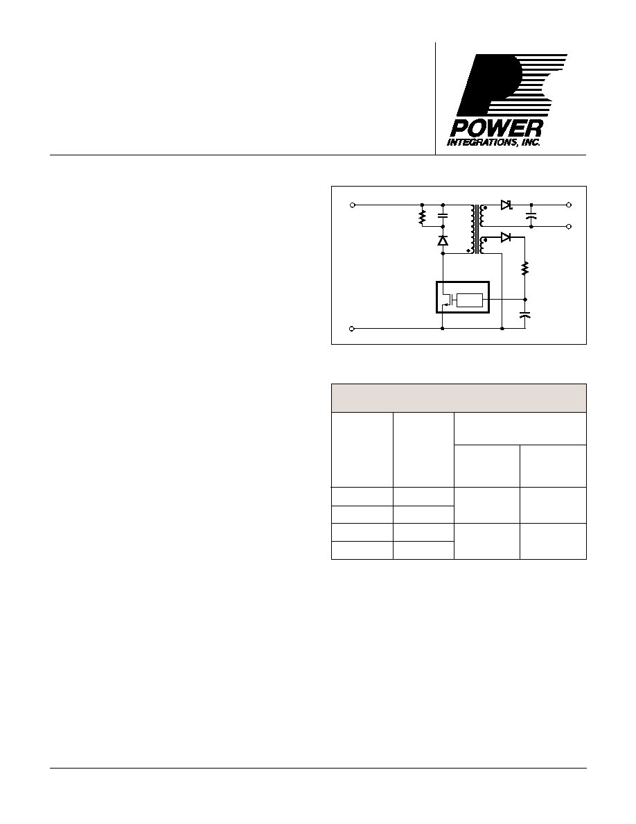
Figure 1. Typical Application.
TOP209/210
TOPSwitch
Family
Three-terminal Off-line PWM Switch
ORDER
PART
NUMBER
OUTPUT POWER RANGE
Æ
85-265
VAC
230 VAC or
110 VAC
w/Doubler
PI-2043-052397
Wide-Range
DC Input
D
S
C
CONTROL
TOPSwitch
+
-
Product Highlights
Cost Effective Switcher for Low Power Applications
∑ Replaces linear power supplies
∑ Replaces discrete switcher and 20 to 50 components
≠ cuts cost, increases reliability
∑ Stand-by power supplies for Green or energy efficient
products such as personal computers, monitors, UPS,
copiers, fax machines, etc.
∑ Housekeeping or "keep-alive" power supply applications
such as TV, appliances, industrial control and personal
computers
∑ Meets 'Blue Angel' low power stand-by specification
∑ Controlled MOSFET turn-on reduces EMI and EMI filter
costs
∑ 80% smaller and lighter compared to linear supply
∑ 50% smaller compared to discrete switcher
Over 80% Efficiency in Flyback Topology
∑ Built-in start-up and current limit reduce DC losses
∑ Low capacitance 700 V MOSFET cuts AC losses
∑ CMOS controller/gate driver consumes only 6 mW
∑ 70% maximum duty cycle minimizes conduction losses
Simplifies Design ≠ Reduces Time to Market
∑ Supported by reference design boards
∑ Integrated PWM Controller and 700 V MOSFET in
industry standard eight pin DIP package
∑ Only one external capacitor needed for compensation,
bypass and start-up/auto-restart functions
∑ Easily interfaces with both opto and primary feedback
System Level Fault Protection Features
∑ Auto-restart and cycle by cycle current limiting functions
handle both primary and secondary faults
∑ On-chip thermal shutdown with hysteresis protects the
entire system against overload
Description
The TOP209/210 implements all functions necessary for an
off-line switched mode control system: high voltage N-channel
power MOSFET with controlled turn-on gate driver, voltage
mode PWM controller with integrated oscillator, high voltage
start-up bias circuit, bandgap derived reference, bias shunt
regulator/error amplifier for loop compensation and fault
protection circuitry. Compared to discrete MOSFET and
controller or self oscillating (RCC) switching converter
solutions, a TOPSwitch integrated circuit can reduce total cost,
component count, size, weight and at the same time increase
efficiency and system reliability. The TOP209/210 are intended
for 100/110/230 VAC off-line Power Supply applications in
the 0 to 8 W (0 to 5 W universal) range.
TOP209P
TOP210PFI
TOPSwitch
Selection Guide
PACKAGE
DIP-8
TOP209G
TOP210G
0-4 W
0-2 W
0-8 W
0-5 W
DIP-8
SMD-8
SMD-8
August
1997
A
8/97
2
TOP209/210
2
PI-1742-011796
SHUTDOWN/
AUTO-RESTART
PWM
COMPARATOR
CLOCK
SAW
OSCILLATOR
CONTROLLED
TURN-ON
GATE
DRIVER
INTERNAL
SUPPLY
5.7 V
4.7 V
SOURCE
S
R
Q
Q
DMAX
-
+
CONTROL
-
+
5.7 V
IFB
RE
ZC
VC
MINIMUM
ON-TIME
DELAY
+
-
VI
LIMIT
LEADING
EDGE
BLANKING
POWER-UP
RESET
˜
8
0
1
THERMAL
SHUTDOWN
WITH
HYSTERESIS
SHUNT REGULATOR/
ERROR AMPLIFIER
+
-
DRAIN
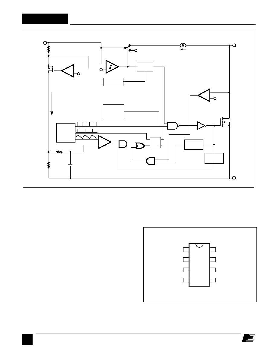
Figure 2. Functional Block Diagram.
Pin Functional Description
DRAIN Pin:
Output MOSFET drain connection. Provides internal bias
current during start-up operation via an internal switched high-
voltage current source. Internal current sense point.
CONTROL Pin:
Error amplifier and feedback current input pin for duty cycle
control. Internal shunt regulator connection to provide internal
bias current during normal operation. It is also used as the
supply bypass and auto-restart/compensation capacitor
connection point.
SOURCE Pin:
Control circuit common, internally connected to output
MOSFET source.
SOURCE (HV RTN) Pin:
Output MOSFET source connection for high voltage return.
PI--2044-040901
CONTROL
8
5
7
6
DRAIN
N/C
N/C
N/C
1
4
2
3
N/C
SOURCE (HV RTN)
SOURCE
P Package (DIP-8)
G Package (SMD-8)
Figure 3. Pin Configuration.
A
8/97
TOP209/210
3
TOPSwitch
Family Functional Description
TOPSwitch is a self biased and protected
linear control current-to-duty cycle
converter with an open drain output.
High efficiency is achieved through the
use of CMOS and integration of the
maximum number of functions possible.
CMOS significantly reduces bias
currents as compared to bipolar or
discrete solutions. Integration eliminates
external power resistors used for current
sensing and/or supplying initial start-up
bias current.
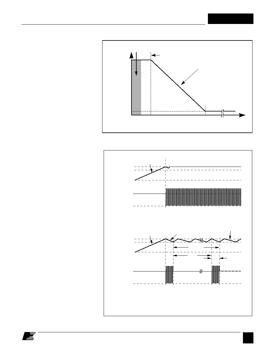
During normal operation, the internal
output MOSFET duty cycle linearly
decreases with increasing CONTROL
pin current as shown in Figure 4. To
implement all the required control, bias,
and protection functions, the DRAIN
and CONTROL pins each perform
several functions as described below.
Refer to Figure 2 for a block diagram
and Figure 6 for timing and voltage
waveforms of the TOPSwitch integrated
circuit.
Control Voltage Supply
CONTROL pin voltage V
C
is the supply
or bias voltage for the controller and
driver circuitry. An external bypass
capacitor closely connected between the
CONTROL and SOURCE pins is
required to supply the gate drive current.
The total amount of capacitance
connected to this pin (C
T
) also sets the
auto-restart timing as well as control
loop compensation. V
C
is regulated in
either of two modes of operation.
Hysteretic regulation is used for initial
start-up and overload operation. Shunt
regulation is used to separate the duty
cycle error signal from the control circuit
supply current. During start-up, V
C
current is supplied from a high-voltage
switched current source connected
internally between the DRAIN and
CONTROL pins. The current source
provides sufficient current to supply the
control circuitry as well as charge the
total external capacitance (C
T
).
PI-2047-060497
DMAX
DMIN
ICD1
Duty Cycle (%)
IC (mA)
2.5
6.5
Slope = PWM Gain
-16%/mA
IB
Auto-restart
Figure 4. Relationship of Duty Cycle to CONTROL Pin Current.
Figure 5. Start-up Waveforms for (a) Normal Operation and (b) Auto-restart.
DRAIN
0
VIN
VC
0
4.7 V
5.7 V
8 Cycles
95%
5%
Off
Switching
Switching
Off
IC
Charging CT
ICD1
Discharging CT
ICD2
Discharging CT
IC
Charging CT
Off
PI-1124A-060694
DRAIN
0
VIN
VC
0
4.7 V
5.7 V
Off
Switching
(b)
(a)
C
T
is the total external capacitance
connected to the CONTROL pin

A
8/97
4
TOP209/210
2
The first time V
C
reaches the upper threshold, the high-voltage
current source is turned off and the PWM modulator and output
transistor are activated, as shown in Figure 5(a). During normal
operation (when the output voltage is regulated) feedback
control current supplies the V
C
supply current. The shunt
regulator keeps V
C
at typically 5.7 V by shunting CONTROL
pin feedback current exceeding the required DC supply current
through the PWM error signal sense resistor R
E
. The low
dynamic impedance of this pin (Z
C
) sets the gain of the error
amplifier when used in a primary feedback configuration. The
dynamic impedance of the CONTROL pin together with the
external resistance and capacitance determines the control loop
compensation of the power system.
If the CONTROL pin external capacitance (C
T
) should discharge
to the lower threshold, then the output MOSFET is turned off
and the control circuit is placed in a low-current standby mode.
The high-voltage current source is turned on and charges the
external capacitance again. Charging current is shown with a
negative polarity and discharging current is shown with a
positive polarity in Figure 6. The hysteretic auto-restart
comparator keeps V
C
within a window of typically 4.7 to 5.7 V
by turning the high-voltage current source on and off as shown
in Figure 5(b). The auto-restart circuit has a divide-by-8
counter which prevents the output MOSFET from turning on
again until eight discharge-charge cycles have elapsed. The
counter effectively limits TOPSwitch power dissipation by
reducing the auto-restart duty cycle to typically 5%. Auto-
restart continues to cycle until output voltage regulation is
again achieved.
Bandgap Reference
All critical TOPSwitch internal voltages are derived from a
temperature-compensated bandgap reference. This reference
is also used to generate a temperature-compensated current
source which is trimmed to accurately set the oscillator frequency
and MOSFET gate drive current.
Oscillator
The internal oscillator linearly charges and discharges the
internal capacitance between two voltage levels to create a
sawtooth waveform for the pulse width modulator. The oscillator
sets the pulse width modulator/current limit latch at the beginning
of each cycle. The nominal frequency of 100 kHz was chosen
to minimize EMI and maximize efficiency in power supply
applications. Trimming of the current reference improves
oscillator frequency accuracy.
Pulse Width Modulator
The pulse width modulator implements a voltage-mode control
loop by driving the output MOSFET with a duty cycle inversely
proportional to the current flowing into the CONTROL pin.
The error signal across R
E
is filtered by an RC network with a
typical corner frequency of 7 kHz to reduce the effect of
switching noise. The filtered error signal is compared with the
internal oscillator sawtooth waveform to generate the duty
cycle waveform. As the control current increases, the duty
cycle decreases. A clock signal from the oscillator sets a latch
which turns on the output MOSFET. The pulse width modulator
resets the latch, turning off the output MOSFET. The maximum
duty cycle is set by the symmetry of the internal oscillator. The
modulator has a minimum ON-time to keep the current
consumption of the TOPSwitch independent of the error signal.
Note that a minimum current must be driven into the CONTROL
pin before the duty cycle begins to change.
Gate Driver
The gate driver is designed to turn the output MOSFET on at a
controlled rate to minimize common-mode EMI. The gate drive
current is trimmed for improved accuracy.
Error Amplifier
The shunt regulator can also perform the function of an error
amplifier in primary feedback applications. The shunt regulator
voltage is accurately derived from the temperature compensated
bandgap reference. The gain of the error amplifier is set by the
CONTROL pin dynamic impedance. The CONTROL pin
clamps external circuit signals to the V
C
voltage level. The
CONTROL pin current in excess of the supply current is
separated by the shunt regulator and flows through R
E
as the
error signal.
Cycle-By-Cycle Current Limit
The cycle by cycle peak drain current limit circuit uses the
output MOSFET ON-resistance as a sense resistor. A current
limit comparator compares the output MOSFET ON-state drain-
source voltage, V
DS(ON)
, with a threshold voltage. High drain
current causes V
DS(ON)
to exceed the threshold voltage and turns
the output MOSFET off until the start of the next clock cycle.
The current limit comparator threshold voltage is temperature
compensated to minimize variation of the effective peak current
limit due to temperature related changes in output MOSFET
R
DS(ON)
.
The leading edge blanking circuit inhibits the current limit
comparator for a short time after the output MOSFET is turned
on. The leading edge blanking time has been set so that current
spikes caused by primary-side capacitances and secondary-side
rectifier reverse recovery time will not cause premature
termination of the switching pulse.
TOPSwitch
Family Functional Description (cont.)
A
8/97
TOP209/210
5
PI-1742-011796
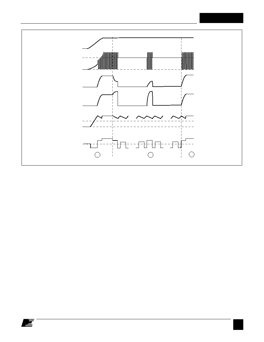
VIN
VOUT
0
IOUT
0
1
2
1
DRAIN
0
VIN
VC
0
∑ ∑ ∑
∑ ∑ ∑
1
2
1
2
8
1
0
IC
∑ ∑ ∑
∑ ∑ ∑
1
2
8
8
1
2
8
1
Shutdown/Auto-restart
To minimize TOPSwitch power dissipation, the shutdown/
auto-restart circuit turns the power supply on and off at a duty
cycle of typically 5% if an out of regulation condition persists.
Loss of regulation interrupts the external current into the
CONTROL pin. V
C
regulation changes from shunt mode to the
hysteretic auto-restart mode described above. When the fault
condition is removed, the power supply output becomes
regulated, V
C
regulation returns to shunt mode, and normal
operation of the power supply resumes.
Hysteretic Overtemperature Protection
Temperature protection is provided by a precision analog
circuit that turns the output MOSFET off when the junction
temperature exceeds the thermal shutdown temperature
(typically 145
∞C). When the junction temperature cools past
the hysteresis temperature, normal operation resumes. V
C
is
regulated in hysteretic mode while the power supply is turned
off.
High-voltage Bias Current Source
This current source biases TOPSwitch from the DRAIN pin and
charges the CONTROL pin external capacitance (C
T
) during
start-up or hysteretic operation. The current source is switched
on and off with an effective duty cycle of approximately 35%.
This duty cycle is determined by the ratio of CONTROL pin
charge (I
C
) and discharge currents (I
CD1
and I
CD2
). This current
source is turned off during normal operation when the output
MOSFET is switching.
Figure 6. Typical Waveforms for (1) Normal Operation, (2) Auto-restart.