 | –≠–ª–µ–∫—Ç—Ä–æ–Ω–Ω—ã–π –∫–æ–º–ø–æ–Ω–µ–Ω—Ç: TOP246 | –°–∫–∞—á–∞—Ç—å:  PDF PDF  ZIP ZIP |
Æ
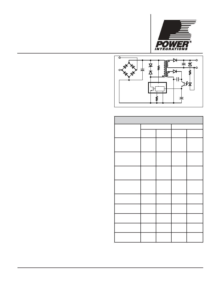
Figure 1. Typical Flyback Application.
PRODUCT
3
Adapter
1
Open
Frame
2
Open
Frame
2
OUTPUT POWER TABLE
Table 1. Notes: 1. Typical continuous power in a non-ventilated
enclosed adapter measured at 50
∞C ambient. 2. Maximum practical
continuous power in an open frame design at 50
∞C ambient. See
Key Applications for detailed conditions. 3. See Part Ordering
Information. 4. 230 VAC or 100/115 VAC with doubler.
230 VAC
±
15%
4
Adapter
1
85-265 VAC
9 W
15 W
6.5 W
10 W
21 W
22 W
11 W
14 W
10 W
22 W
7 W
14 W
13 W
25 W
9 W
15 W
29 W
45 W
17 W
23 W
20 W
45 W
15 W
30 W
16 W
28 W
11 W
20 W
34 W
50 W
20 W
28 W
30 W
65 W
20 W
45 W
19 W
30 W
13 W
22 W
37 W
57 W
23 W
33 W
40 W
85 W
26 W
60 W
40 W
64 W
26 W
38 W
60 W
125 W
40 W
90 W
42 W
70 W
28 W
43 W
85 W
165 W
55 W
125 W
43 W
75 W
30 W
48 W
105 W
205 W
70 W
155 W
44 W
79 W
31 W
53 W
120 W
250 W
80 W
180 W
45 W
82 W
32 W
55 W
135 W
290 W
90 W
210 W
Product Highlights
Lower System Cost, High Design Flexibility
∑ Extended power range for higher power applications
∑ No heatsink required up to 30 W using P package
∑ Features eliminate or reduce cost of external components
∑ Fully integrated soft-start for minimum stress/overshoot
∑ Externally programmable accurate current limit
∑ Wider duty cycle for more power, smaller input capacitor
∑ Separate line sense and current limit pins on Y/R/F packages
∑ Line under-voltage (UV) detection: no turn off glitches
∑ Line overvoltage (OV) shutdown extends line surge limit
∑ Line feed forward with maximum duty cycle (DC
MAX
)
reduction rejects line ripple and limits DC
MAX
at high line
∑ Frequency jittering reduces EMI and EMI filtering costs
∑ Regulates to zero load without dummy loading
∑ 132 kHz frequency reduces transformer/power supply size
∑ Half frequency option in Y/R/F packages for video applications
∑ Hysteretic thermal shutdown for automatic fault recovery
∑ Large thermal hysteresis prevents PC board overheating
EcoSmart
- Energy Efficient
∑ Extremely low consumption in remote off mode
(80 mW @ 110 VAC, 160 mW @ 230 VAC)
∑ Frequency lowered with load for high standby efficiency
∑ Allows shutdown/wake-up via LAN/input port
Description
TOPSwitch-GX uses the same proven topology as TOPSwitch, cost
effectively integrating the high voltage power MOSFET, PWM
control, fault protection and other control circuitry onto a single
CMOS chip. Many new functions are integrated to
reduce system cost and improve design flexibility, performance
and energy efficiency.
Depending on package type, either 1 or 3 additional pins over the
TOPSwitch standard DRAIN, SOURCE and CONTROL terminals
allow the following functions: line sensing (OV/UV, line feed-
forward/DC
MAX
reduction), accurate externally set current limit,
remote ON/OFF, synchronization to an external lower frequency,
and frequency selection (132 kHz/66 kHz).
All package types provide the following transparent features: Soft-
start, 132 kHz switching frequency (automatically reduced at light
load), frequency jittering for lower EMI, wider DC
MAX
, hysteretic
thermal shutdown and larger creepage packages. In addition, all
critical parameters (i.e. current limit, frequency, PWM gain) have
tighter temperature and absolute tolerance, to simplify design and
optimize system cost.
TOP242 P or G
TOP242 R
TOP242 Y or F
TOP243 P or G
TOP243 R
TOP243 Y or F
TOP244 P or G
TOP244 R
TOP244 Y or F
TOP245 P
TOP245 R
TOP245 Y or F
TOP246 R
TOP246 Y or F
TOP247 R
TOP247 Y or F
TOP248 R
TOP248 Y or F
TOP249 R
TOP249 Y or F
TOP250 R
TOP250 Y or F
Æ
TOP242-250
TOPSwitch
-
GX
Family
Extended Power, Design Flexible,
EcoSmart
,
Integrated
Off-line Switcher
September 2003
PI-2632-060200
AC
IN
DC
OUT
D
S
C
TOPSwitch-GX
CONTROL
L
+
-
F
X

TOP242-250
2
K
9/03
General Information & Table of Contents
Product Selector Guide 1
Data Sheets 2
Application Notes 3
Design Ideas 4
Design Tools 5
Quality and Reliability 6
Package Information 7
DPA-Switch DC-DC Seminar 8
LinkSwitch & TinySwitch-II AC-DC Seminar 9
TOPSwitch-GX AC-DC Seminar 10
Sales Representatives and Distributors 11
Section List
Functional Block Diagram ......................................................................................................................................... 3
Pin Functional Description ........................................................................................................................................ 4
TOPSwitch-GX Family Functional Description ........................................................................................................ 5
CONTROL (C) Pin Operation ................................................................................................................................. 6
Oscillator and Switching Frequency ....................................................................................................................... 6
Pulse Width Modulator and Maximum Duty Cycle ................................................................................................. 7
Light Load Frequency Reduction ............................................................................................................................ 7
Error Amplifier ......................................................................................................................................................... 7
On-chip Current Limit with External Programmability ............................................................................................. 7
Line Under-Voltage Detection (UV) ........................................................................................................................ 8
Line Overvoltage Shutdown (OV) ........................................................................................................................... 8
Line Feed Forward with DC
MAX
Reduction .............................................................................................................. 8
Remote ON/OFF and Synchronization ................................................................................................................... 9
Soft-Start ................................................................................................................................................................ 9
Shutdown/Auto-Restart .......................................................................................................................................... 9
Hysteretic Over-Temperature Protection ................................................................................................................ 9
Bandgap Reference .............................................................................................................................................. 10
High-Voltage Bias Current Source ........................................................................................................................ 10
Using Feature Pins .................................................................................................................................................... 10
FREQUENCY (F) Pin Operation ........................................................................................................................... 10
LINE-SENSE (L) Pin Operation ............................................................................................................................ 10
EXTERNAL CURRENT LIMIT (X) Pin Operation ................................................................................................. 11
MULTI-FUNCTION (M) Pin Operation .................................................................................................................. 11
Typical Uses of FREQUENCY (F) Pin ...................................................................................................................... 14
Typical Uses of LINE-SENSE (L) and EXTERNAL CURRENT LIMIT (X) Pins ....................................................... 15
Typical Uses of MULTI-FUNCTION (M) Pin ............................................................................................................. 17
Application Examples ............................................................................................................................................... 20
A High Efficiency, 30 W, Universal Input Power Supply ........................................................................................ 20
A High Efficiency, Enclosed, 70 W, Universal Adapter Supply .............................................................................. 21
A High Efficiency, 250 W, 250-380 VDC Input Power Supply ............................................................................... 22
Multiple Output, 60 W, 185-265 VAC Input Power Supply .................................................................................... 23
Processor Controlled Supply Turn On/Off ............................................................................................................ 24
Key Application Considerations .............................................................................................................................. 26
TOPSwitch-II vs. TOPSwitch-GX .......................................................................................................................... 26
TOPSwitch-FX vs. TOPSwitch-GX ....................................................................................................................... 27
TOPSwitch-GX Design Considerations ................................................................................................................ 28
TOPSwitch-GX Layout Considerations ................................................................................................................. 30
Quick Design Checklist ......................................................................................................................................... 30
Design Tools ......................................................................................................................................................... 32
Product Specifications and Test Conditions .......................................................................................................... 33
Typical Performance Characteristics ...................................................................................................................... 40
Part Ordering Information ........................................................................................................................................ 45
Package Outlines ...................................................................................................................................................... 45

TOP242-250
3
K
9/03
Figure 2a. Functional Block Diagram (Y, R or F Package).
Figure 2b. Functional Block Diagram (P or G Package).
PI-2639-060600
SHUTDOWN/
AUTO-RESTART
PWM
COMPARATOR
CLOCK
SAW
HALF
FREQ.
CONTROLLED
TURN-ON
GATE DRIVER
CURRENT LIMIT
COMPARATOR
INTERNAL UV
COMPARATOR
INTERNAL
SUPPLY
5.8 V
4.8 V
SOURCE (S)
S
R
Q
DMAX
STOP SOFT-
START
-
+
CONTROL (C)
LINE-SENSE (L)
EXTERNAL
CURRENT LIMIT (X)
FREQUENCY (F)
-
+
5.8 V
1 V
IFB
RE
ZC
VC
+
-
LEADING
EDGE
BLANKING
˜
8
1
HYSTERETIC
THERMAL
SHUTDOWN
SHUNT REGULATOR/
ERROR AMPLIFIER
+
-
DRAIN (D)
ON/OFF
SOFT
START
DCMAX
VBG
DCMAX
VBG + VT
0
OV/UV
VI (LIMIT)
CURRENT
LIMIT
ADJUST
LINE
SENSE
SOFT START
LIGHT LOAD
FREQUENCY
REDUCTION
STOP LOGIC
OSCILLATOR WITH JITTER
PI-2641-061200
SHUTDOWN/
AUTO-RESTART
PWM
COMPARATOR
CLOCK
SAW
CONTROLLED
TURN-ON
GATE DRIVER
CURRENT LIMIT
COMPARATOR
INTERNAL UV
COMPARATOR
INTERNAL
SUPPLY
5.8 V
4.8 V
SOURCE (S)
S
R
Q
DMAX
STOP SOFT-
START
-
+
CONTROL (C)
MULTI-
FUNCTION (M)
-
+
5.8 V
IFB
RE
ZC
VC
+
-
LEADING
EDGE
BLANKING
˜
8
1
HYSTERETIC
THERMAL
SHUTDOWN
SHUNT REGULATOR/
ERROR AMPLIFIER
+
-
DRAIN (D)
ON/OFF
SOFT
START
DCMAX
VBG
DCMAX
VBG + VT
0
OV/UV
VI (LIMIT)
CURRENT
LIMIT
ADJUST
LINE
SENSE
SOFT START
LIGHT LOAD
FREQUENCY
REDUCTION
STOP LOGIC
OSCILLATOR WITH JITTER
TOP242-250
4
K
9/03
General Information & Table of Contents
Product Selector Guide 1
Data Sheets 2
Application Notes 3
Design Ideas 4
Design Tools 5
Quality and Reliability 6
Package Information 7
DPA-Switch DC-DC Seminar 8
LinkSwitch & TinySwitch-II AC-DC Seminar 9
TOPSwitch-GX AC-DC Seminar 10
Sales Representatives and Distributors 11
Pin Functional Description
DRAIN (D) Pin:
High voltage power MOSFET drain output. The internal
start-up bias current is drawn from this pin through a switched
high-voltage current source. Internal current limit sense point
for drain current.
CONTROL (C) Pin:
Error amplifier and feedback current input pin for duty cycle
control. Internal shunt regulator connection to provide internal
bias current during normal operation. It is also used as the
connection point for the supply bypass and auto-restart/
compensation capacitor.
LINE-SENSE (L) Pin: (Y, R or F package only)
Input pin for OV, UV, line feed forward with DC
MAX
reduction,
remote ON/OFF and synchronization. A connection to
SOURCE pin disables all functions on this pin.
EXTERNAL CURRENT LIMIT (X) Pin: (Y, R or F
package only)
Input pin for external current limit adjustment, remote
ON/OFF, and synchronization. A connection to SOURCE pin
disables all functions on this pin.
MULTI-FUNCTION (M) Pin: (P or G package only)
This pin combines the functions of the LINE-SENSE (L) and
EXTERNAL CURRENT LIMIT (X) pins of the Y package
into one pin. Input pin for OV, UV, line feed forward with
DC
MAX
reduction, external current limit adjustment, remote
ON/OFF and synchronization. A connection to SOURCE pin
disables all functions on this pin and makes TOPSwitch-GX
operate in simple three terminal mode (like TOPSwitch-II).
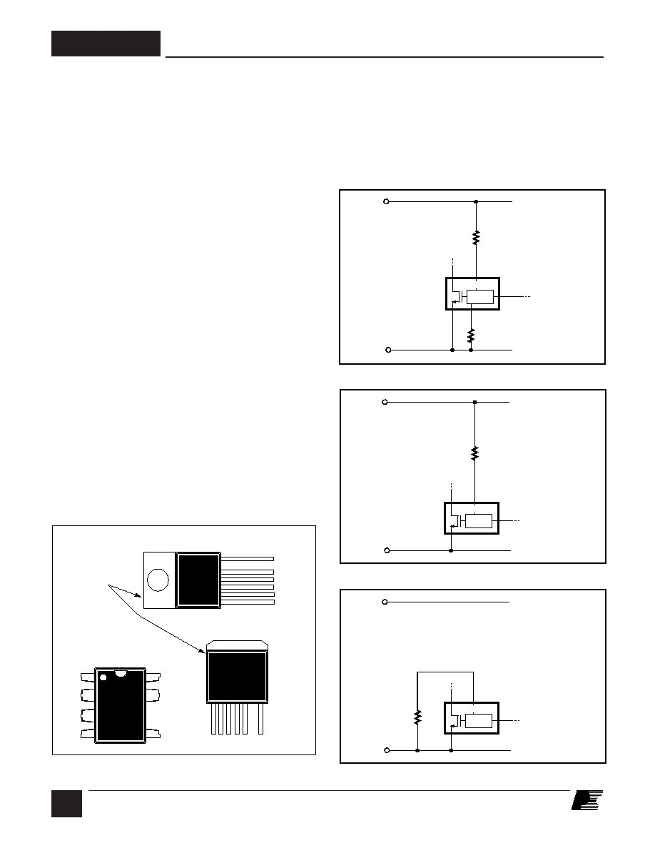
Figure 3. Pin Configuration (top view).
PI-2509-040501
DC
Input
Voltage
+
-
D
M
S
C
V
UV
= I
UV
x R
LS
V
OV
=
I
OV
x
R
LS
For R
LS
= 2 M
V
UV
= 100 VDC
V
OV
=
450 VDC
DC
MAX
@100 VDC = 78%
DC
MAX
@375 VDC = 38%
CONTROL
R
LS
2 M
Figure 4. Y/R/F Pkg Line Sense and Externally Set Current Limit.
Figure 5. P/G Package Line Sense.
Figure 6. P/G Package Externally Set Current Limit.
FREQUENCY (F) Pin: (Y, R or F package only)
Input pin for selecting switching frequency: 132 kHz if
connected to SOURCE pin and 66 kHz if connected to
CONTROL pin. The switching frequency is internally set for
fixed 132 kHz operation in P and G packages.
SOURCE (S) Pin:
Output MOSFET source connection for high voltage power
return. Primary side control circuit common and reference point.
PI-2724-010802
Tab Internally
Connected to
SOURCE Pin
Y Package (TO-220-7C)
C
D
S
S
S
S
1 C
3 X
2 L
5 F
4 S
7 D
M
P Package (DIP-8B)
G Package (SMD-8B)
R Package (TO-263-7C)
F Package (TO-262-7C)
8
5
7
1
1 2 3 4 5
7
C L X S F
D
4
2
3
X
PI-2629-092203
DC
Input
Voltage
+
-
D
S
C
CONTROL
L
R
IL
R
LS
12 k
2 M
V
UV
= I
UV
x R
LS
V
OV
=
I
OV
x
R
LS
For R
LS
= 2 M
DC
MAX
@100 VDC = 78%
DC
MAX
@375 VDC = 38%
For R
IL
= 12 k
I
LIMIT
= 69%
See Figure 54b for
other resistor values
(R
IL
) to select different
I
LIMIT
values
V
UV
= 100 VDC
V
OV
= 450 VDC
PI-2517-092203
DC
Input
Voltage
+
-
D
M
S
C
For R
IL
= 12 k
I
LIMIT
= 69%
CONTROL
R
IL
See Figures 54b and
55b for other resistor
values (R
IL
) to select
different I
LIMIT
values
For R
IL
= 25 k
I
LIMIT
= 43%

TOP242-250
5
K
9/03
TOPSwitch-GX
Family Functional Description
The pin can also be used as a remote ON/OFF and a
synchronization input.
The EXTERNAL CURRENT LIMIT (X) pin is usually used to
reduce the current limit externally to a value close to the operating
peak current, by connecting the pin to SOURCE through a resistor.
This pin can also be used as a remote ON/OFF and a
synchronization input in both modes. See Table 2 and Figure 11.
For the P or G packages the LINE-SENSE and EXTERNAL
CURRENT LIMIT pin functions are combined on one MULTI-
FUNCTION (M) pin. However, some of the functions become
mutually exclusive as shown in Table 3.
The FREQUENCY (F) pin in the Y, R or F package sets the
switching frequency to the default value of 132 kHz when
connected to SOURCE pin. A half frequency option of 66 kHz
can be chosen by connecting this pin to CONTROL pin
instead. Leaving this pin open is not recommended.
PI-2633-011502
Duty Cycle (%)
I
C
(mA)
TOP242-5 1.6 2.0
TOP246-9 2.2 2.6
TOP250 2.4 2.7
5.2 6.0
5.8 6.6
6.5 7.3
I
CD1
I
B
Auto-restart
I
L
= 125
µ
A
I
L
< I
L(DC)
I
L
= 190
µ
A
78
10
38
Frequency (kHz)
I
C
(mA)
30
I
CD1
I
B
Auto-restart
132
Note: For P and G packages I
L
is replaced with I
M
.
I
L
< I
L(DC)
I
L
= 125
µ
A
Slope = PWM Gain
I
L
= 190
µ
A
Figure 7. Relationship of Duty Cycle and Frequency to CONTROL
Pin Current.
Like TOPSwitch, TOPSwitch-GX is an integrated switched
mode power supply chip that converts a current at the control
input to a duty cycle at the open drain output of a high voltage
power MOSFET. During normal operation the duty cycle of
the power MOSFET decreases linearly with increasing
CONTROL pin current as shown in Figure 7.
In addition to the three terminal TOPSwitch features, such as
the high voltage start-up, the cycle-by-cycle current limiting,
loop compensation circuitry, auto-restart, thermal shutdown,
the TOPSwitch-GX incorporates many additional functions that
reduce system cost, increase power supply performance and
design flexibility. A patented high voltage CMOS technology
allows both the high voltage power MOSFET and all the low
voltage control circuitry to be cost effectively integrated onto
a single monolithic chip.
Three terminals, FREQUENCY, LINE-SENSE, and
EXTERNAL CURRENT LIMIT (available in Y, R or F
package) or one terminal MULTI-FUNCTION (available in P
or G package) have been added to implement some of the new
functions. These terminals can be connected to the SOURCE
pin to operate the TOPSwitch-GX in a TOPSwitch-like three
terminal mode. However, even in this three terminal mode, the
TOPSwitch-GX offers many new transparent features that do
not require any external components:
1. A fully integrated 10 ms soft-start limits peak currents and
voltages during start-up and dramatically reduces or
eliminates output overshoot in most applications.
2. DC
MAX
of 78% allows smaller input storage capacitor, lower
input voltage requirement and/or higher power capability.
3. Frequency reduction at light loads lowers the switching
losses and maintains good cross regulation in multiple
output supplies.
4. Higher switching frequency of 132 kHz reduces the
transformer size with no noticeable impact on EMI.
5. Frequency jittering reduces EMI.
6. Hysteretic over-temperature shutdown ensures automatic
recovery from thermal fault. Large hysteresis prevents circuit
board overheating.
7. Packages with omitted pins and lead forming provide large
drain creepage distance.
8. Tighter absolute tolerances and smaller temperature vari-
ations on switching frequency, current limit and PWM gain.
The LINE-SENSE (L) pin is usually used for line sensing by
connecting a resistor from this pin to the rectified DC high
voltage bus to implement line overvoltage (OV), under-voltage
(UV) and line feed-forward with DC
MAX
reduction. In this
mode, the value of the resistor determines the OV/UV thresholds
and the DC
MAX
is reduced linearly starting from a line voltage
above the under-voltage threshold. See Table 2 and Figure 11.