
ULC0402FC3.3C
thru
ULC0402FC36C
1
05152.R7 4/05
www.protekdevices.com
UNBUMPED LOW CAPACITANCE FLIP CHIP ARRAY
Only One Name Means ProTek'TionTM
APPLICATIONS
Cellular Phones
Personal Digital Assistant (PDA)
Notebook Computers
SMART Cards
IEC COMPATIBILITY (EN61000-4)
61000-4-2 (ESD): Air - 15kV, Contact - 8kV
61000-4-4 (EFT): 40A - 5/50ns
FEATURES
ESD Protection > 25 kilovolts
Available in Voltages Ranging From 3.3V to 36V
200 Watts Peak Pulse Power per Line (tp = 8/20µs)
Low Clamping Voltage
Bidirectional Configuration & Monolithic Structure
Protects 1 Line
LOW CAPACITANCE
LOW LEAKAGE CURRENT
RoHS Compliant
MECHANICAL CHARACTERISTICS
Standard EIA Chip Size: 0402
Weight 0.73 milligrams (Approximate)
Solder Reflow Temperature:
Tin-Lead - Sn/Pb: 240-245∞C
Lead-Free: 260-270∞C
Flammability Rating UL 94V-0
8mm Plastic & Paper Tape and Reel Per EIA Standard 481
Device Marking On Reel
U0402
05152
PIN CONFIGURATION
2
www.protekdevices.com
05152.R7 4/05
ULC0402FC3.3C
thru
ULC0402FC36C
DEVICE CHARACTERISTICS
MAXIMUM RATINGS @ 25∞C Unless Otherwise Specified
Operating Temperature
SYMBOL
VALUE
-55
∞
C to 150
∞
C
∞C
∞C
-55
∞
C to 150
∞
C
UNITS
T
J
T
STG
PARAMETER
Storage Temperature
Peak Pulse Power (t
p
= 8/20µs) - See Figure 1
P
PP
200
Watts
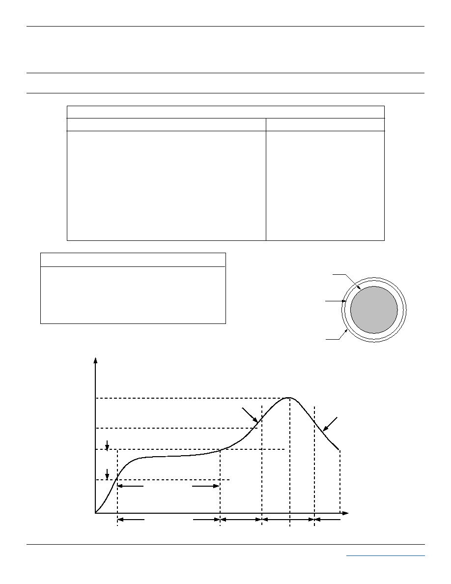
0 5 10 15 20 25 30
t - Time - µs
0
20
40
60
80
100
120
I
PP
- Peak Pulse Current - % of I
PP
TEST
WAVEFORM
PARAMETERS
t
f
= 8µs
t
d
= 20µs
t
f
Peak Value I
PP
e
-t
t
d
= t
I
PP
/2
FIGURE 2
PULSE WAVE FORM
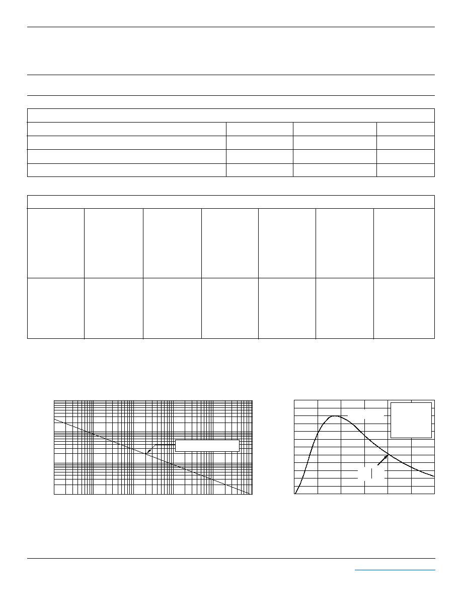
0.01 1 10 100 1,000 10,000
t
d
- Pulse Duration - µs
10
100
1,000
10,000
P
PP
- Peak Pulse Current - Watts
FIGURE 1
PEAK PULSE POWER VS PULSE TIME
200W, 8/20µs Waveform
ELECTRICAL CHARACTERISTICS PER LINE @ 25∞C Unless Otherwise Specified
PART
NUMBER
(See Note 1)
MINIMUM
BREAKDOWN
VOLTAGE
@ 1mA
V
(BR)
VOLTS
MAXIMUM
CLAMPING
VOLTAGE
(See Fig. 2)
@ I
P
= 1A
V
C
VOLTS
MAXIMUM
CLAMPING
VOLTAGE
(See Fig. 2)
@8/20µs
V
C
@ I
PP
TYPICAL
CAPACITANCE
@0V, 1 MHz
C
pF
ULC0402FC3.3C
ULC0402FC05C
ULC0402FC08C
ULC0402FC12C
ULC0402FC15C
ULC0402FC24C
ULC0402FC36C
3.3
5.9
8.0
12.0
15.0
24.0
36.0
4.0
6.0
8.5
13.3
16.7
26.7
40.0
7.0
11.0
13.2
19.8
25.4
37.2
70.0
12.5V @ 16A
13V @ 15A
18V @ 11A
26.9V @ 7.4A
34.5V @ 5.8A
50.6V @ 4A
80.0V @ 2.5A
70
35
32
30
25
20
18
MAXIMUM
LEAKAGE
CURRENT
(See Note 2)
@V
WM
I
D
µA
75*
10**
1
1
1
1
1
RATED
STAND-OFF
VOLTAGE
V
WM
VOLTS
Note 1:
All devices are bidirectional. Electrical characteristics apply in both directions.
Note 2:
*Maximum leakage current < 5µA @ 2.8V. **Maximum leakage current <500nA @ 3.3V.

3
www.protekdevices.com
05152.R7 4/05
ULC0402FC3.3C
thru
ULC0402FC36C
GRAPHS
0 5 10 15 20
V
C
- Clamping
V
oltage -
V
olts
0
4
8
12
14
FIGURE 5
TYPICAL CLAMPING VOLTAGE VS PEAK PULSE CURRENT FOR ULC0402FC05C
10
6
2
I
PP
- Peak Pulse Current - Amps
ESD Test Pulse - 25 kilovolt, 1/30ns (waveshape)
FIGURE 4
OVERSHOOT & CLAMPING VOLTAGE FOR ULC0402FC05C
5
V
o
lts per Division
-5
5
15
25
35
0 25 50 75 100 125 150
T
L
- Lead Temperature - ∞C
20
40
60
80
100
% Of Rated Power
Peak Pulse Power
8/20µs
Average Power
FIGURE 3
POWER DERATING CURVE
0
4
www.protekdevices.com
05152.R7 4/05
ULC0402FC3.3C
thru
ULC0402FC36C
Ramp-up
Ramp-down
Ramp-up
15 seconds
Solder Time
15-20 seconds
Ramp-down
T
S
- Preheat
T
SMAX
T
SMIN
T
L
t 25∞C to Peak
30-60 seconds
T
emperature - ∞C
T
P
155∞
140∞
0.275mm
Round
Non-Solder Mask Defined Pads
0.325mm Round
0.150mm
0.330mm Round
No Clean
OSP(Entek Cu Plus 106A)
±50µm
±20µm
60 Seconds
270∞C
Pad Size on PCB
Pad Shape
Pad Definition
Solder Mask Opening
Solder Stencil Thickness
Solder Stencil Aperture Opening (laser cut, 5% tapered walls)
Solder Paste Type
Pad Protective Finish
Tolerance - Edge To Corner Ball
Solder Ball Side Coplanarity
Maximum Dwell Time Above Liquidous (183∞C)
Soldering Maximum Temperature
PRINTED CIRCUIT BOARD RECOMMENDATIONS
PARAMETER
VALUE
REQUIREMENTS
Temperature:
T
P
for Lead-Free (SnAgCu): 260-265∞C
T
P
for Tin-Lead: 240-245∞C
Preheat time and temperature depends on solder paste and flux
activation temperature, component size, weight, surface area &
plating.
RECOMMENDED NON-SOLDER MASK
DEFINED PAD ILLUSTRATION
Non-Solder Mask Defined Pad
0.275mm DIA.
Solder Mask Opening
0.325mm DIA.
Solder Stencil Opening
0.330mm DIA.
APPLICATION INFORMATION
5
www.protekdevices.com
05152.R7 4/05
ULC0402FC3.3C
thru
ULC0402FC36C
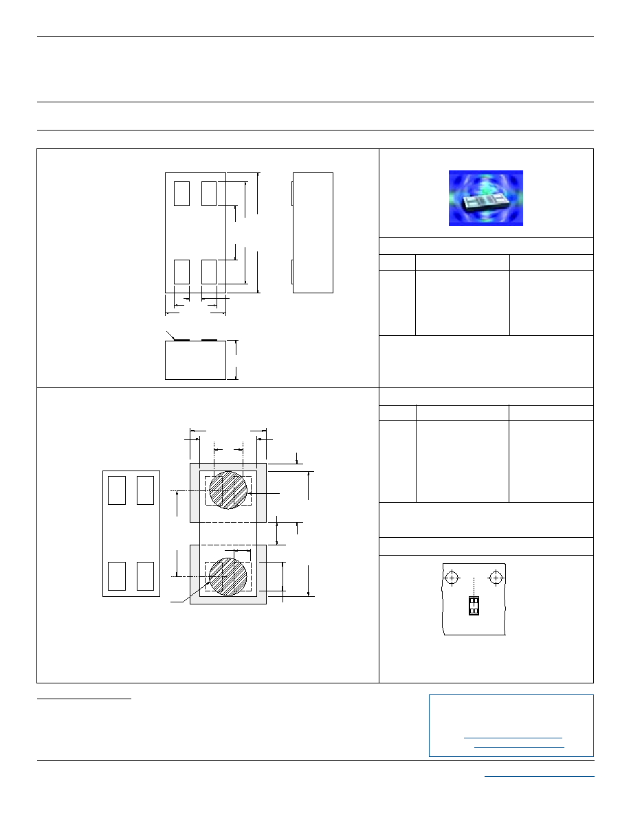
PACKAGE OUTLINE & DIMENSIONS
TAPE & REEL ORDERING NOMENCLATURE
1. Surface mount product is taped and reeled in accordance with EIA 481.
2.
8mm Plastic Tape: 7 Inch Reels - 5,000 pieces per reel. Ordering Suffix: -T75-1 (i.e., ULC0402FC05C-T75-1).
3.
8mm Paper Tape: 7 Inch Reels -10,000 pieces per reel. Ordering Suffix: -T710-2 (i.e., ULC0402FC05C-T710-2).
A
B
C
D
E
F
I
0.46 NOM
0.86 NOM
0.99 ± 0.0254
0.10 NOM
0.35 NOM
0.483 ± 0.0254
0.406 NOM
0.018 NOM
0.034 NOM
0.039 ± 0.001
0.004 NOM
0.014 NOM
0.019 ± 0.001
0.016 NOM
DIM
MILLIMETERS
INCHES
PACKAGE DIMENSIONS
NOTES:
1. Controlling dimensions in inches.
2. Decimal tolerances for mounting pad and outline:
.xxx ± 0.05mm (± 0.002").
3. Maximum chip size: 1.02 (0.040") by 0.51(0.020").
PACKAGE OUTLINE
U0402
MOUNTING PAD
NOTE:
1.
Preferred: Using 0.1mm (0.004") stencil.
D
E
F
I
SIDE
A
B
C
TOP
END
Metalized Die Contacts
A
B
C
D
E
F
G
H
I
0.23
0.48
0.69
0.46
0.99
0.20
0.20
0.66
0.13
0.009
0.019
0.027
0.018
0.039
0.008
0.008
0.026
0.005
DIM
MILLIMETERS
INCHES
PAD DIMENSIONS
NOTE:
1. Top view of tape. Metal contacts are face down in tape
package.
TAPE & REEL ORIENTATION
Single Die - 0402
B
C
DIE
CONTACTS
A
H
D
I
SOLDER PRINT
DIAMETER 0.010" -
0.012"
F
G
DIE
E
SOLDER P
A
D
Outline & Dimensions: Rev 3 - 11/02, 06020
ProTek Devices
2929 South Fair Lane, Tempe, AZ 85282
Tel: 602-431-8101 Fax: 602-431-2288
E-Mail:
sales@protekdevices.com
Web Site:
www.protekdevices.com
COPYRIGHT © ProTek Devices 2005
SPECIFICATIONS: ProTek reserves the right to change the electrical and or mechanical characteristics described herein without notice (except JEDEC).
DESIGN CHANGES: ProTek reserves the right to discontinue product lines without notice, and that the final judgement concerning selection and
specifications is the buyer's and that in furnishing engineering and technical assistance, ProTek assumes no responsibility with respect to the selection or
specifications of such products.