251
www.ptcc.com.tw
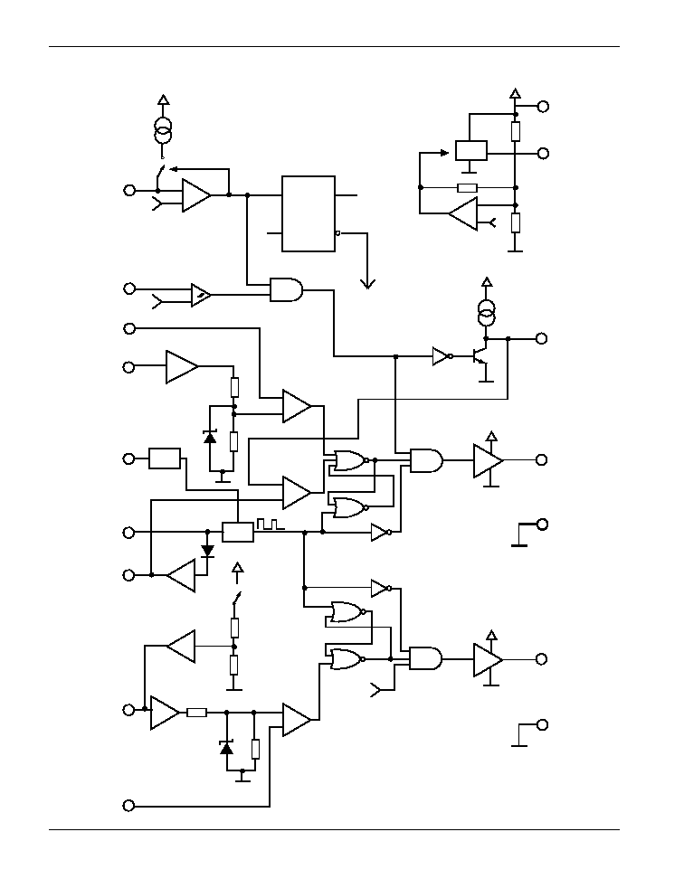
AS2916
PWM Controller
Pin Function Description
Pin Number
Function
Description
1
OUTB
This is the gate drive output for the Main FET. The totem pole
output has equivalent of an extra 10
resistor to limit the FET
turn on speed and a pull down resistor to ensure the FET gate
is never open. No external circuitry except for the FET is
expected on this pin. The largest FET expected to be driven is
IRFBC40. If a larger power FET is used, a buffer might be
required.
2
VCC
Positive supply for the IC. Absolute maximum rating is 20 V.
The running voltage shall be provided by the Auxiliary conver
tor.
3
REG
Output of 5 V series regulator.
4
SNSB
This is the Main convertor current sense pin. An external RC
filter from the Main power FET and slope compensation resis-
tor from the RAMP pin is all the expected external circuitry.
5
CMPB
This is the Main output control pin. An opto isolated control
signal from the secondary side error amplifier is buffered and
connected to the invert pin of the main output current mode
comparator. A pull-up current of 1 mA is provided so the only
external circuitry expected is a common emitter opto-isolator.
6
SS
This pin provides a 6 µA current source to linearly charge an
external capacitor. This spin is compared to the RAMP pin in
the soft start comparator, terminating output pulses when
RAMP goes above the SS voltage. While this pin is held low,
the main output is inhibited.
7
RAMP
This pin is a level-shifted and buffered oscillator waveform,
used to provide slope compensation for the Main and Auxiliary
converters. The pin also serves as the non-inverting input of
the soft-start comparator.
8
OSC
Oscillator frequency and maximum duty cycle are set by con-
necting the resistor (RT) to VREG and a capacitor (CT) to
ground.
9
WBL
Provides an FM modulation of the oscillator, approximately
±25% deviation frequency, at a modulation rate set by an exter-
nal cap at WBL. Shorting to GND eliminates modulation.
10
ON
This pin is used to remotely turn the main convertor ON/OFF
either for normal user application or for protection.
11
BOK
Bulk OK. This is a brownout protection feature. The pin moni-
tors the bulk voltage through a resistor divider. When BOK
exceeds 2.5 V a 50 µA current is sourced from the pin for hys-
teresis. When the pin drops below 2.5 V the hysteresis is
turned off and SS is pulled low,inhibiting the main output.
The Auxiliary output is not tied to BOK and will run as long as
there is sufficient bias voltage.

252
www.ptcc.com.tw
AS2916
PWM Controller
Pin Function Description
Pin Number
Function
Description
12
CMPA
This is the Auxiliary convertor error amplifier compensation pin
or if secondary controller is desired, the Auxiliary control input
pin. A simple capacitor to ground is the only circuitry expected.
Note: There is no external connection for voltage feedback.
Voltage sensing is provided internally in such a way that VCC
is
not loaded until it reaches predefined threshold. If secondary
control is required, it can be forced into the CMPA pin.
13
SNSA
This is the Auxiliary convertor current sense pin. An external
RC filter from the Auxiliary power FET and slope compensation
resistor from the RAMP pin is all the expected external cir-
cuitry.
14
OUTA
This is the gate drive output for the Auxiliary FET. The totem
pole output has equivalent of an extra 33
resistor to limit the
FET turn on speed and a pull down resistor to ensure the FET
gate is never open. No external circuitry except for the FET is
expected on this pin. The largest FET expected to be driven is
IRF820. If a larger power FET is used, a buffer might be
required.
15
GND
Signal ground.
16
PGND
Power ground.
Absolute Maximum Ratings
Parameter
Symbol
Rating
Unit
Reference Current
IREF
200
mA
Output Current
IOUT
1
A
Supply Voltage
VCC
20
V
Output Voltage
VOUT
20
V
Continuous Power
PD
500
mW
Junction Temperature
TJ
150
∞C
Storage Temperature
TSTG
≠60 to +150
∞C
Lead Temperature (Soldering, 10 seconds)
TL
300
∞C

253
www.ptcc.com.tw
AS2916
PWM Controller
Electrical Characteristics
Electrical characteristics are guaranteed over the full junction temperature range (0-105∞). Ambient temperature must be derated
based upon power dissipation and package thermal characteristics. The conditions are: VCC = 15 V, BOK = 3 V, ON = 3 V, RT =
680
, CT = 10 nF, and CWBL = 2.2 nF, unless otherwise specified. To override UVLO, VCC should be raised above UVLOHIGH
prior to test.
Parameter
Symbol
Test Condition
Min.
Typ.
Max.
Unit
5 V Regulator
Output Voltage
VREG
TJ = 25∞C, IREG = 1 mA
4.90
5.00
5.10
V
Line Regulation
PSRR
12
VCC
18 V
5
15
mV
Load Regulation
1.0
IREG
20 mA
5
15
mV
Temperature Stability
TCREG
0.2
0.4
mV/∞C
Total Output Variation
Line, Load, Temperature
4.85
5.15
V
Long-Term Stability
Over 1,000 hrs at 25∞C
5.0
25
mV
Output Noise Voltage
VNOISE
10
f
100 kHz, TJ = 25∞C
50
µV
Maximum Source Current
IMAX
VREG = 4.8 V
30
120
180
mA
Oscillator
Initial Frequency
fOSC
TA = 25∞C, VWBL = 0 V
117
132
143
kHz
Voltage Stability
8.5 V
VCC
18V
0.2
1.0
%
Temperature Stability
TCF
TMIN
TJ
TMAX
5
%
Amplitude
VOSC
VOSC peak-to-peak
1.55
V
Upper Trip Point
VH
VWBL = 0 V
2.8
V
Lower Trip Point
VL
VWBL = 0 V
1.25
V
Discharge Current
IDSC
VOSC = 3 V
7.5
8.7
9.5
mA
Duty Cycle Limit
RT = 680
, CT = 10 nF,
46
50
54
%
TJ = 25∞C
Over-Temperature Shutdown
TOT
140
∞C
Wobble Oscillator
Wobble Rate
FWBL
2.2 nF WBL to GND
3.4
4.5
6.0
kHz
OSC Frequency Deviation
DEV
Change in main oscillator freq.
+30
+40
+50
kHz
Amplitude
VWBL
VWBL peak-to-peak
1.8
V
Upper Trip Point
VH
2.7
V
Lower Trip Point
VL
0.9
V
Charge Current
ICHRG
VWBL = 0.7 V
≠25
≠36
≠50
µA
Discharge Current
IDSC
VWBL = 4.8 V
25
36
50
µA