
13
P4C147
P4C147
ULTRA HIGH SPEED 4K x 1
STATIC CMOS RAM
FEATURES
Full CMOS, 6T Cell
High Speed (Equal Access and Cycle Times)
≠ 10/12/15/20/25 ns (Commercial)
≠ 15/20/25/35 ns (Military)
Low Power Operation
≠ 715 mW Active
≠10 (Commercial)
≠ 550 mW Active
≠25 (Commercial)
≠ 110 mW Standby (TTL Input)
≠ 55 mW Standby (CMOS Input)
Single 5V
±
10% Power Supply
Separate Input and Output Ports
Three-State Outputs
Fully TTL Compatible Inputs and Outputs
Standard Pinout (JEDEC Approved)
≠ 18 Pin 300 mil DIP
≠ 18 Pin CERPACK
≠ 18 Pin LCC (290 x 430 mils)
DESCRIPTION
The P4C147 is a 4,096-bit ultra high speed static RAM
organized as 4K x 1. The CMOS memories require no
clocks or refreshing, and have equal access and cycle
times. Inputs are fully TTL-compatible. The RAM operates
from a single 5V
±
10% tolerance power supply.
Access times as fast as 10 nanoseconds are available,
permitting greatly enhanced system operating speeds.
CMOS is utilized to reduce power consumption in both
active and standby modes. In addition to very high
performance, this device features latch-up protection and
single-event-upset protection.
The P4C147 is available in 18 pin 300 mil DIP packages
as well as an 18-pin CERPACK package and LCC.
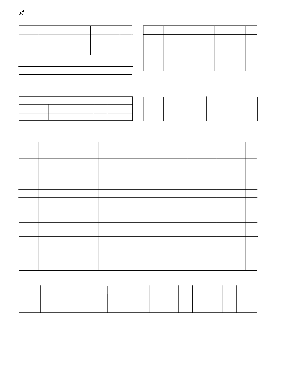
CE
WE
INPUT
DATA
CONTROL
ROW
SELECT
COLUMN
SELECT
4,096-BIT
MEMORY
ARRAY
COLUMN I/O
D
OUT
D
IN
A
A
A
A
DIP (P1, D1), CERPACK (F1) SIMILAR
LCC (L7)
TOP VIEW
(6)
(6)
1Q97
Means Quality, Service and Speed
FUNCTIONAL BLOCK DIAGRAM
PIN CONFIGURATIONS
A2
DOUT
GN
D
3
7
9
A6
WE
CE
D
IN
10
11
12
13
14
15
1
2
4
5
6
8
16
17
18
A3
A4
A5
A7
A8
A9
A10
A
0
A
1
V
CC
A
11
A11
A10
A9
A8
A7
A6
A4
A0
A1
A2
A3
A5
VCC
CE
GND
DOUT
WE
1
2
3
4
5
6
7
8
9
18
17
16
15
14
13
12
11
10
DIN
14
P4C147
MAXIMUM RATINGS
(1)
Symbol
Parameter
Value
Unit
V
CC
Power Supply Pin with
≠ 0.5 to +7
V
Respect to GND
Terminal Voltage with
≠ 0.5 to
V
TERM
Respect to GND
V
CC
+0.5
V
(up to 7.0V)
T
A
Operating Temperature
≠ 55 to +125
∞
C
Symbol
Parameter
Value
Unit
T
BIAS
Temperature Under
≠ 55 to +125
∞
C
Bias
T
STG
Storage Temperature
≠ 65 to +150
∞
C
P
T
Power Dissipation
1.0
W
I
OUT
DC Output Current
50
mA
CAPACITANCES
(4)
(V
CC
= 5.0V, T
A
= 25
∞
C, f = 1.0MHz)
Grade
(2)
Commercial
Military
Symbol
Parameter
Conditions Typ. Unit
C
IN
Input Capacitance
V
IN
= 0V
5
pF
C
OUT
Output Capacitance V
OUT
= 0V
7
pF
Ambient Temp
0∞C to 70∞C
-55∞C to +125∞C
Gnd
0V
0V
V
CC
5.0V
±
10%
5.0V
±
10%
RECOMMENDED OPERATING
CONDITIONS
V
OH
V
OL
V
IH
V
IL
I
LI
I
LO
I
SB
I
SB1
Parameter
Symbol
Output High Voltage
(TTL Load)
Output Low Voltage
(TTL Load)
Input High Voltage
Input Low Voltage
Input Leakage Current
Output Leakage Current
Standby Power Supply
Current (TTL Input Levels)
Standby Power Supply
Current
(CMOS Input Levels)
Test Conditions
I
OH
= ≠4 mA, V
CC
= Min.
I
OL
= +8 mA, V
CC
= Min
V
CC
= Max., V
IN
= GND to V
CC
CE
V
IH
, V
CC
= Max., Mil.
f=Max., Output Open Comm'l
CE
V
HC
, V
CC
= Max., f= 0, Mil.
Output Open Comm'l
V
IN
0.2V or V
IN
V
CC
-0.2V
P4C147
Min.
2.4
2.2
≠0.5
(3)
__
__
__
__
DC ELECTRICAL CHARACTERISTICS
Over recommended operating temperature and supply voltage (2)
Max.
V
CC
=+0.5
0.8
30
23
15
10
Unit
V
V
V
mA
mA
µ
A
µ
A
V
0.4
Symbol
Parameter
Dynamic Operating Current
Unit
-35
-25
-20
-15
-12
Commercial
Military
Temperature
Range
I
CC
POWER DISSIPATION CHARACTERISTICS VS. SPEED
130
N/A
130
N/A
120
145
115
135
100
125
N/A
120
mA
mA
-10
Mil.
Comm'l
≠10
≠5
+10
+5
Mil.
Comm'l
≠10
≠5
+10
+5
V
CC
= Max.,
CE
= V
IH
,
V
OUT
= GND to V
CC
15
P4C147
Min
Notes:
1. Stresses greater than those listed under MAXIMUM RATINGS may
cause permanent damage to the device. This is a stress rating only
and functional operation of the device at these or any other conditions
above those indicated in the operational sections of this specification
is not implied. Exposure to MAXIMUM rating conditions for extended
periods may affect reliability.
2. Extended temperature operation guaranteed with 400 linear feet per
minute of air flow.
3. Transient inputs with V
IL
and I
IL
not more negative than ≠3.0V and
≠100mA, respectively, are permissible for pulse widths up to 20 ns.
4. This parameter is sampled and not 100% tested.
5.
CE
is LOW and
WE
is HIGH for READ cycle.
6.
WE
is HIGH, and address must be valid prior to or coincident with
CE
transition LOW.
7. Transition is measured
±
200mV from steady state voltage prior to
change with specified loading in Figure 1. This parameter is sampled
and not 100% tested.
8. Read Cycle Time is measured from the last valid address to the first
transitioning address.
t
CE
DATA OUT
AC
t
RC
t
LZ
DATA VALID
I
CC
I
SB
t
PU
HIGH IMPEDANCE
t
PD
(7)
(7)
t
HZ
SUPPLY
CC
CURRENT
V
TIMING WAVEFORM OF READ CYCLE NO. 2
(6)
ADDRESS
DATA OUT
t
AA
DATA VALID
PREVIOUS DATA VALID
(8)
t
OH
t
RC
TIMING WAVEFORM OF READ CYCLE NO. 1
(5)
Sym.
t
RC
t
AA
t
AC
t
HZ
t
PU
t
PD
Read Cycle Time
Chip Enable Access Time
Output Hold from
Address Change
Chip Enable to
Output in Low Z
Chip Disable to
Output in High Z
Chip Enable to
Power Up Time
Chip Disable to
Power Down Time
-10
-12
-15
-20
-25
-35
Unit
ns
ns
ns
ns
ns
ns
ns
ns
Min
Max
10
10
4
10
10
2
2
0
AC CHARACTERISTICS--READ CYCLE
(V
CC
= 5V
±
10%, All Temperature Ranges)
(2)
12
2
2
0
Max
12
12
5
12
Min
15
2
2
0
Max
15
15
6
15
Min
20
2
2
0
Max
20
20
8
20
Min
25
2
2
0
Max
25
25
10
25
Min
35
2
2
0
Max
35
35
14
35
Parameter
Address Access Time
t
OH
t
LZ

16
P4C147
Notes:
9.
CE
and
WE
must be LOW for WRITE cycle.
10. If
CE
goes HIGH simultaneously with
WE
high, the output remains
in a high impedance state.
11. Write Cycle Time is measured from the last valid address to the first
transition address.
-10
TIMING WAVEFORM OF WRITE CYCLE NO. 1 (
WE
WE
WE
WE
WE
CONTROLLED)
(9)
ADDRESS
CE
t
WC
DATA VALID
HIGH IMPEDANCE
WE
DATA IN
DATA OUT
DATA UNDEFINED
(11)
(12)
t
CW
t
AW
t
WP
t
DW
t
WR
t
AH
t
DH
t
OW
t
AS
t
WZ
(10, 12)
12. Transition is measured
±
200mV from steady state voltage prior to
change with specified loading in Figure 1. This parameter is
sampled and not 100% tested.
TIMING WAVEFORM OF WRITE CYCLE NO. 2 (
CE
CE
CE
CE
CE
CONTROLLED)
(9)
t
t
WE
ADDRESS
CE
DATA OUT
DATA IN
t
WC
DATA VALID
HIGH IMPEDANCE
(11)
t
AS
t
CW
t
AW
t
WP
DW
AH
WR
t
DH
t
Sym.
t
WC
t
CW
t
AW
t
AS
t
WP
t
AH
t
DW
t
DH
t
WZ
t
OW
Parameter
Chip Enable Time to End of Write
Address Valid to End of Write
Address Set-up Time
Write Pulse Width
Address Hold Time from
End of Write
Data Valid to End of Write
Data Hold Time
Write Enable to Output in High Z
Output Active from End of Write
Min
10
8
8
0
8
0
5
0
0
Max
5
-12
Min
12
10
10
0
10
0
6
0
0
Max
6
-15
Min
15
12
12
0
12
0
7
0
0
Max
7
-20
Min
20
15
15
0
14
0
9
0
0
Max
9
-25
Min
25
20
20
0
15
0
12
0
0
Max
12
AC CHARACTERISTICS--WRITE CYCLE
(V
CC
= 5V
±
10%, All Temperature Ranges)
(2)
-35
Min
35
25
25
0
18
0
15
0
0
Max
15
Unit
ns
ns
ns
ns
ns
ns
ns
ns
ns
ns
Write Cycle Time
17
P4C147
Input Pulse Levels
GND to 3.0V
Input Rise and Fall Times
3ns
Input Timing Reference Level
1.5V
Output Timing Reference Level
1.5V
Output Load
See Figures 1 and 2
Mode
CE
CE
CE
CE
CE
WE
WE
WE
WE
WE
Output
Power
Standby
H
X
High Z
Standby
Read
L
H
D
OUT
Active
Write
L
L
High Z
Active
TRUTH TABLE
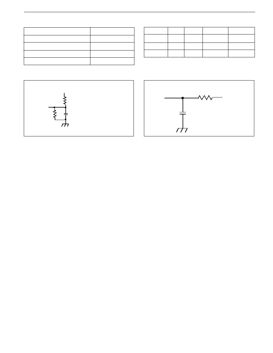
AC TEST CONDITIONS
Figure 1. Output Load
Figure 2. Thevenin Equivalent
* including scope and test fixture.
Note:
Due to the ultra-high speed of the P4C147, care must be taken when
testing this device; an inadequate setup can cause a normal functioning
part to be rejected as faulty. Long high-inductance leads that cause
supply bounce must be avoided by bringing the V
CC
and ground planes
directly up to the contactor fingers. A 0.01
µ
F high frequency capacitor
is also required between V
CC
and ground. To avoid signal reflections,
proper termination must be used; for example, a 50
test environment
should be terminated into a 50
load with 1.73V (Thevenin Voltage) at
the comparator input, and a 116
resistor must be used in series with
D
OUT
to match 166
(Thevenin Resistance).
RTH = 166.5
VTH = 1.73 V
DOUT
30pF (5pF* for tHZ, tLZ, tOHZ,
tOLZ, tWZ and tOW)
DOUT
255
480
+5
30pF (5pF* for tHZ, tLZ, tOHZ,
tOLZ, tWZ and tOW)