91
P4C164/164L
FEATURES
Full CMOS, 6T Cell
High Speed (Equal Access and Cycle Times)
≠ 8/10/12/15/20/25 ns (Commercial)
≠ 10/12/15/20/25/35 (Industrial)
≠ 12/15/20/25/35/45 ns (Military)
Low Power Operation
≠ 770mW Active ≠15
≠ 660/743 mW Active ≠ 20
≠ 495/575 mW Active ≠ 25, 35, 45
≠ 193/220 mW Standby (TTL Input)
≠ 5.5mW Standby (CMOS Input) P4C164L (Military)
Output Enable and Dual Chip Enable Control
Functions
Single 5V
±
10% Power Supply
Data Retention with 2.0V Supply, 10
µ
A Typical
Current (P4C164L Military)
Common Data I/O
Fully TTL Compatible Inputs and Outputs
Standard Pinout (JEDEC Approved)
≠ 28-Pin 300 mil DIP, SOJ
≠ 28-Pin 600 mil Ceramic DIP
≠ 28-Pin 350 x 550 mil LCC
≠ 28-Pin CERPACK
P4C164/P4C164L
ULTRA HIGH SPEED 8K x 8
STATIC CMOS RAMS
DESCRIPTION
The P4C164 and P4C164L are 65,536-bit ultra high-speed
static RAMs organized as 8K x 8. The CMOS memories
require no clocks or refreshing and have equal access and
cycle times. Inputs are fully TTL-compatible. The RAMs
operate from a single 5V
±
10% tolerance power supply.
With battery backup, data integrity is maintained with
supply voltages down to 2.0V. Current drain is typically 10
µ
A from a 2.0V supply.
Access times as fast as 10 nanoseconds are available,
permitting greatly enhanced system operating speeds. In
full standby mode with CMOS inputs, power consumption
is only 5.5 mW for the P4C164L.
The P4C164 and P4C164L are available in 28-pin 300 mil
DIP and SOJ, 28-pin 600 mil ceramic DIP, and 28-pin 350
x 550 mil LCC packages providing excellent board level
densities.
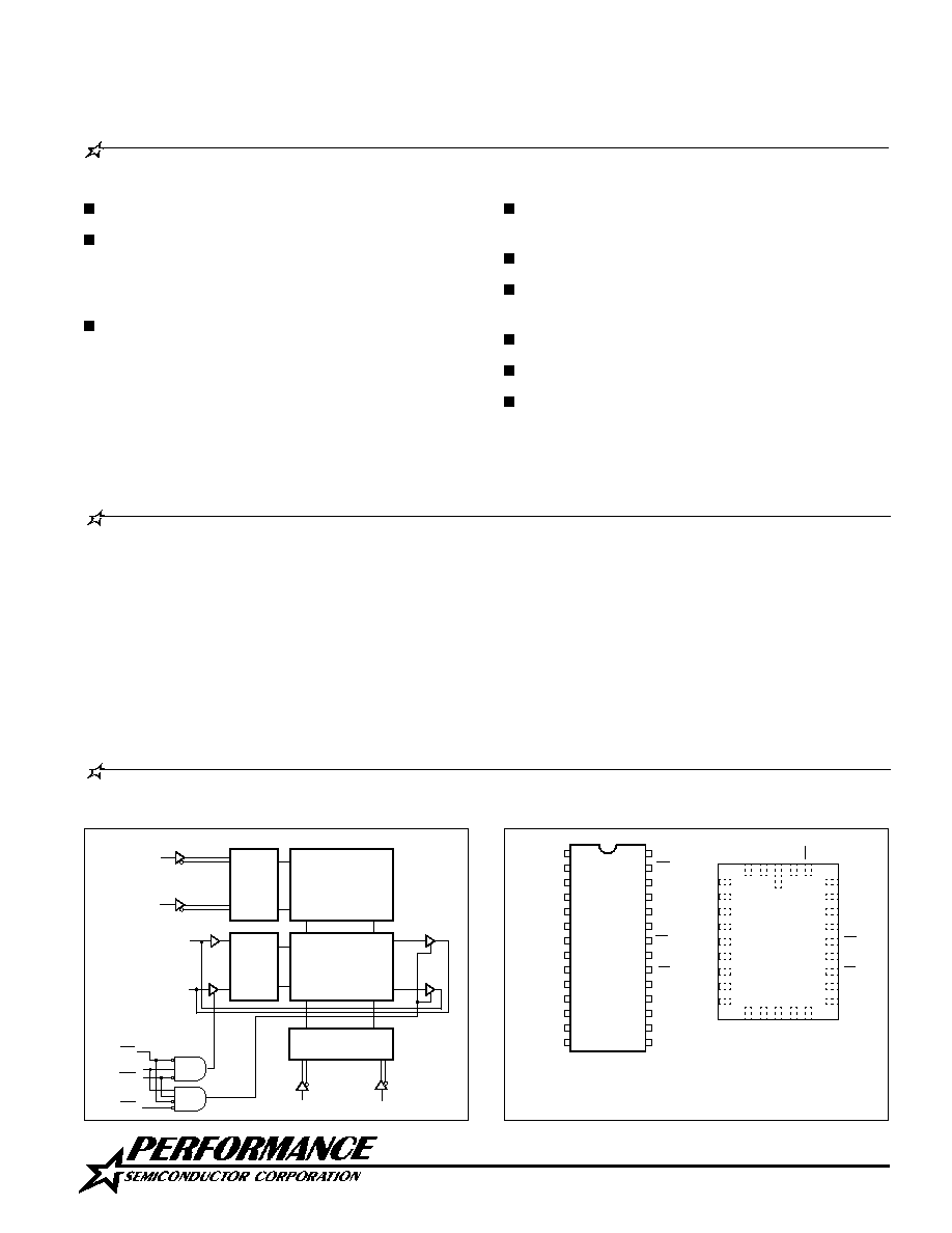
FUNCTIONAL BLOCK DIAGRAM
PIN CONFIGURATIONS
1519B
A
0
NC
A
2
A
3
A
4
A
5
A
6
A
7
A
8
CE
1
2
3
4
5
6
7
8
9
10
11
12
13
14
28
27
26
25
24
23
22
21
20
19
18
17
16
15
A
11
A
9
CE
2
I/O
I/O
I/O
1519B
GND
WE
10
A
A
12
OE
V
CC
1
2
3
1
I/O
8
I/O
7
I/O
I/O
5
I/O
4
6
A
1
A
2
NC
A
4
A
5
A
6
A
7
A
8
I/O
1
CE
CE
2
A
12
A
11
A
10
GND
A
0
A
1
V
CC
26
25
24
23
22
21
20
4
5
6
7
8
9
10
11
12
19
18
13
17
3
27
1
15
2
14
28
16
I/O
2
A
9
OE
I/O
8
I/O
7
WE
I/O
3
I/O
4
I/O
5
I/O
6
A
3
1
1519C
1519A
INPUT
DATA
CONTROL
ROW
SELECT
65,536-BIT
MEMORY
ARRAY
COLUMN I/O
I/O
1
I/O
8
COLUMN
SELECT
WE
OE
A
0
A
7
A
8
A
12
CE
1
CE
2
∑ ∑ ∑ ∑ ∑ ∑
∑ ∑ ∑
∑ ∑ ∑
∑ ∑ ∑
∑ ∑ ∑ ∑ ∑ ∑
1Q97
Means Quality, Service and Speed
LCC (L5)
TOP VIEW
DIP (P5, D5-2, D5-1), SOJ (J5)
CERPACK (F4) SIMILAR
TOP VIEW

92
P4C164/164L
MAXIMUM RATINGS
(1)
Symbol
Parameter
Value
Unit
V
CC
Power Supply Pin with
≠0.5 to +7
V
Respect to GND
Terminal Voltage with
≠0.5 to
V
TERM
Respect to GND
V
CC
+0.5
V
(up to 7.0V)
T
A
Operating Temperature
≠55 to +125
∞
C
Symbol
Parameter
Value
Unit
T
BIAS
Temperature Under
≠55 to +125
∞
C
Bias
T
STG
Storage Temperature
≠65 to +150
∞
C
P
T
Power Dissipation
1.0
W
I
OUT
DC Output Current
50
mA
RECOMMENDED OPERATING
TEMPERATURE AND SUPPLY VOLTAGE
I
SB
Standby Power Supply
Current (TTL Input Levels)
CE
V
IH
or Mil.
CE
2
V
IL
, V
CC
= Max Ind./Com'l.
f = Max., Outputs Open
___
___
40
30
___
___
___
___
25
15
40
n/a
1
n/a
mA
mA
___
___
CE
V
HC
or Mil.
CE
2
V
LC
, V
CC
= Max Ind./Com'l.
f = 0, Outputs Open
V
IN
V
LC
or V
IN
V
HC
Standby Power Supply
Current
(CMOS Input Levels)
I
SB1
Grade(2)
Ambient
Temperature
GND
V
CC
0V
0V
5.0V
±
10%
5.0V
±
10%
0V
5.0V
±
10%
≠55
∞
C to +125
∞
C
Military
Symbol
C
IN
C
OUT
Parameter
Input Capacitance
Output Capacitance
Conditions
V
IN
= 0V
V
OUT
= 0V
5
7
Unit
pF
pF
CAPACITANCES
(4)
V
CC
= 5.0V, T
A
= 25
∞
C, f = 1.0MHz
n/a = Not Applicable
Symbol
DC ELECTRICAL CHARACTERISTICS
Over recommended operating temperature and supply voltage
(2)
V
IH
V
IL
V
HC
V
LC
V
CD
V
OL
V
OH
I
LI
I
LO
Parameter
Input High Voltage
Input Low Voltage
CMOS Input High Voltage
CMOS Input Low Voltage
Input Clamp Diode Voltage
Output Low Voltage
(TTL Load)
Output High Voltage
(TTL Load)
Input Leakage Current
Output Leakage Current
Test Conditions
V
CC
= Min., I
IN
= 18 mA
I
OL
= +8 mA, V
CC
= Min.
I
OH
= ≠4 mA, V
CC
= Min.
V
CC
= Max. Mil.
V
IN
= GND to V
CC
Com'l.
V
CC
= Max.,
CE
= V
IH
, Mil.
V
OUT
= GND to V
CC
Com'l.
P4C164
Min
2.2
≠0.5
(3)
V
CC
≠0.2
≠0.5
(3)
2.4
≠10
≠5
≠10
≠5
Max
V
CC
+0.5
0.8
V
CC
+0.5
0.2
≠1.2
0.4
+10
+5
+10
+5
P4C164L
Min
Max
2.2
≠0.5
(3)
V
CC
≠0.2
≠0.5(3)
2.4
≠5
n/a
≠5
n/a
V
CC
+0.5
0.8
V
CC
+0.5
0.2
0.4
≠1.2
+5
n/a
+5
n/a
Unit
V
V
V
V
V
V
V
µ
A
µ
A
Notes:
1. Stresses greater than those listed under MAXIMUM RATINGS may
cause permanent damage to the device. This is a stress rating only
and functional operation of the device at these or any other conditions
above those indicated in the operational sections of this specification
is not implied. Exposure to MAXIMUM rating conditions for extended
periods may affect reliability.
2. Extended temperature operation guaranteed with 400 linear feet per
minute of air flow.
3. Transient inputs with V
IL
and I
IL
not more negative than ≠3.0V and
≠100mA, respectively, are permissible for pulse widths up to 20 ns.
4. This parameter is sampled and not 100% tested.
Typ.
Industrial
Commercial
≠40
∞
C to +85
∞
C
0
∞
C to +70
∞
C
93
P4C164/164L
DATA RETENTION CHARACTERISTICS (P4C164L, Military Temperature Only)
Typ.*
Max
Symbol
Parameter
Test Condition
Min
V
CC
=
V
CC
=
Unit
2.0V
3.0V
2.0V
3.0V
V
DR
V
CC
for Data Retention
2.0
V
I
CCDR
Data Retention Current
10
15
200
300
µ
A
t
CDR
Chip Deselect to
0
ns
Data Retention Time
t
R
Operation Recovery Time
t
RC
ß
ns
*
T
A
= +25
∞
C
ß
t
RC
= Read Cycle Time
This parameter is guaranteed but not tested.
I
CC
Symbol
Parameter
Temperature
Range
Dynamic Operating Current*
Commercial
Industrial
Military
N/A
N/A
≠10
N/A
≠8
≠12
≠15
≠20
≠25
≠35
≠45
Unit
N/A
mA
mA
mA
*V
CC
= 5.5V. Tested with outputs open. f = Max. Switching inputs are 0V and 3V.
CE
1
= V
IL
, CE
2
= V
IH
,
OE
= V
IH
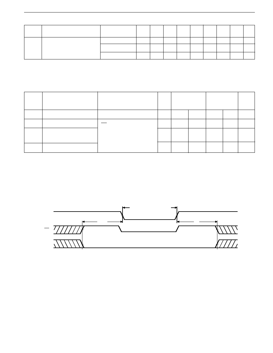
POWER DISSIPATION CHARACTERISTICS VS. SPEED
V
CC
t
CDR
4.5V
V
DR
2V
4.5V
t
R
DATA RETENTION MODE
V
HC
V
DR
CE
CE
1
2
V
LC
V
HC
V
LC
DATA RETENTION WAVEFORM
CE
1
V
CC
≠ 0.2V or
CE
2
0.2V, V
IN
V
CC
≠ 0.2V
or V
IN
0.2V
190
150
155
160
170
180
180
170
160
155
150
145
200
180
170
160
155
150
N/A
N/A

94
P4C164/164L
AC ELECTRICAL CHARACTERISTICS--READ CYCLE
(V
CC
= 5V
±
10%, All Temperature Ranges)
(2)
OLZ
ADDRESS
OE
t
RC
DATA OUT
(9)
t
AA
t
OE
t
OH
CE
CE
1
2
t
LZ
t
AC
t
HZ
t
OHZ
t
(8)
(8)
(8)
(8)
Notes:
5.
WE
is HIGH for READ cycle.
6.
CE
1
is LOW, CE
2
is HIGH and
OE
is LOW for READ cycle.
7. ADDRESS must be valid prior to, or coincident with
CE
1
transition
LOW and CE
2
transition HIGH.
8. Transition is measured
±
200 mV from steady state voltage prior to
change, with loading as specified in Figure 1. This parameter is
sampled and not 100% tested.
READ CYCLE NO. 1 (
OE
OE
OE
OE
OE
CONTROLLED)
(5)
Sym.
t
RC
t
AA
t
AC
t
OH
t
LZ
t
HZ
t
OE
t
OLZ
t
OHZ
t
PU
t
PD
Parameter
Read Cycle Time
Address Access
Time
Chip Enable
Access Time
Output Hold from
Address Change
Chip Enable to
Output in Low Z
Chip Disable to
Output in High Z
Output Enable
Low to Low Z
Output Enable
High to High Z
Chip Enable to
Power Up Time
Chip Disable to
Power Down
Time
Output Enable
Low to Data
Valid
Min Max Min
Max
Min
Max
Min
Max
Min
Max
Min
Max
Min
Max
Min
Max
-12
-15
-20
-25
-35
-45
-8
-10
Unit
8
3
2
0
8
8
2
5
5
5
8
10
3
2
2
0
10
10
6
6
6
10
12
3
2
2
0
12
12
7
7
7
12
15
3
2
2
0
15
15
8
9
9
15
20
3
2
2
0
20
20
8
10
9
20
25
3
2
2
0
25
25
10
13
12
20
35
3
2
2
0
35
35
15
18
15
20
45
3
2
2
0
45
45
20
20
20
25
ns
ns
ns
ns
ns
ns
ns
ns
ns
ns
ns
95
P4C164/164L
t
ADDRESS
DATA OUT
AA
t
t
OH
DATA VALID
PREVIOUS DATA VALID
(9)
RC
READ CYCLE NO. 2 (ADDRESS CONTROLLED)
(5,6)
READ CYCLE NO. 3 (
CE
CE
CE
CE
CE
1
, CE
2
CONTROLLED)
(5,7,10)
Notes:
9. READ Cycle Time is measured from the last valid address to the first
transitioning address.
t
CE
DATA OUT
AC
t
RC
t
LZ
DATA VALID
I
CC
I
SB
t
PU
HIGH IMPEDANCE
t
PD
(8,10)
(8,10)
t
HZ
SUPPLY
CC
CURRENT
V
CE
(10)
(10)
(10)
2
1
10. Transitions caused by a chip enable control have similar delays
irrespective of whether
CE
1
or CE
2
causes them.