99
P4C174
P4C174
HIGH SPEED 8K x 8
CACHE TAG STATIC RAM
1Q97
Means Quality, Service and Speed
FEATURES
High Speed Address-To-Match - 8 ns Maximum
Access Time
High-Speed Read-Access Time
≠ 8/10/12/15/20/25 ns (Commercial)
Open Drain MATCH Output
Reset Function
8-Bit Tag Comparison Logic
Automatic Powerdown During Long Cycles
Data Retention at 2V for Battery Backup Operation
Advanced CMOS Technology
Low Power Operation
-- Active: 750 mW Typical at 25 ns
-- Standby: 500
µ
W Typical
Package Styles Available
-- 28 Pin 300 mil Plastic DIP
-- 28 Pin 300 mil Plastic SOJ
Single Power Supply
-- 5V
±
10%
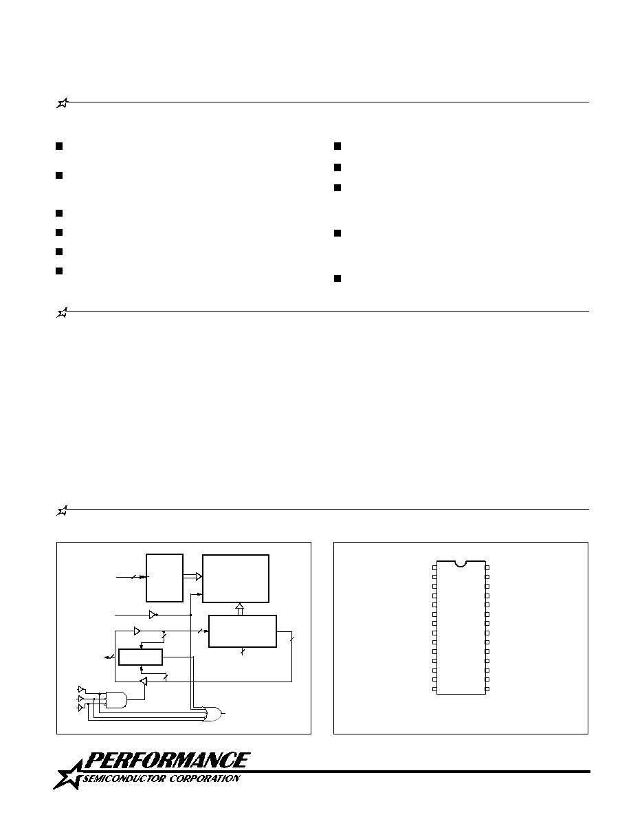
FUNCTIONAL BLOCK DIAGRAM
PIN CONFIGURATION
DESCRIPTION
The P4C174 is a 65,536 bit high speed cache tag static
RAM organized as 8K x 8. The CMOS memory has equal
access and cycle times. Inputs are fully TTL-compatible.
The cache tag RAMs operate from a single 5V
±
10%
power supply. An 8-bit data comparator with a MATCH
output is included for use as an address tag comparator in
high speed cache applications. The reset function pro-
vides the capability to reset all memory locations to a LOW
level.
The MATCH output of the P4C174 reflects the compari-
son result between the 8-bit data on the I/O pins and
the addressed memory location. 8K Cache lines can be
mapped into 1M-Byte address spaces by comparing 20
address bits organized as 13-line address bits and 7-page
address bits.
Low power operation of the P4C174 is enhanced by
automatic powerdown when the memory is deselected or
during long cycle times. Also, data retention is maintained
down to V
CC
= 2.0. Typical battery backup applications
consume only 30
µ
W at V
CC
=
3.0V.
DIP (P5), SOJ (J5)
TOP VIEW
A
10
A
12
1
2
3
4
5
6
7
8
9
10
11
12
13
14
28
27
26
25
24
23
22
21
20
19
18
17
16
15
I/0
0
GND
CE
WE
A
11
OE
Vcc
I/0
1
A
7
A
6
A
5
A
4
A
3
A
2
A
1
A
0
I/0
2
MATCH
A
8
A
9
I/0
7
I/0
6
I/0
5
I/0
4
I/0
3
RESET
ROW
SELECT
256 x 32 x 8
MEMORY
ARRAY
COLUMN SELECT
& COLUMN
SENSE
8
8
RESET
ROW
ADDRESS
8
DATA
I/O
8
COMPARATOR
8
WE
OE
CE
1 (IF MATCH)
5
COLUMN
ADDRESS
8
174.1
MATCH (OPEN DRAIN)

100
P4C174
MAXIMUM RATINGS
(1)
Symbol
Parameter
Value
Unit
V
CC
Power Supply Pin with
≠0.5 to +7
V
Respect to GND
Terminal Voltage with
≠0.5 to
V
TERM
Respect to GND
V
CC
+0.5
V
(up to 7.0V)
T
A
Operating Temperature
≠55 to +125
∞
C
Symbol
Parameter
Value
Unit
T
BIAS
Temperature Under
≠55 to +125
∞
C
Bias
T
STG
Storage Temperature
≠65 to +150
∞
C
P
T
Power Dissipation
1.0
W
I
OUT
DC Output Current
50
mA
RECOMMENDED OPERATING
TEMPERATURE AND SUPPLY VOLTAGE
I
SB
Standby Power Supply
Current (TTL Input Levels)
CE
V
IH
V
CC
= Max .,
f = Max., Outputs Open
___
25
5
___
CE
V
HC
V
CC
= Max.,
f = 0, Outputs Open
V
IN
V
LC
or V
IN
V
HC
Standby Power Supply
Current
(CMOS Input Levels)
I
SB1
Grade(2)
Ambient
Temperature
GND
V
CC
0
∞
C to +70
∞
C
Symbol
C
IN
C
OUT
Parameter
Input Capacitance
Output Capacitance
Conditions
V
IN
= 0V
V
OUT
= 0V
5
7
Unit
pF
pF
CAPACITANCES
(4)
V
CC
= 5.0V, T
A
= 25
∞
C, f = 1.0MHz
n/a = Not Applicable
Symbol
DC ELECTRICAL CHARACTERISTICS
Over recommended operating temperature and supply voltage
(2)
V
IH
V
IL
V
HC
V
LC
V
CD
V
OL
V
OH
I
LI
I
LO
Parameter
Input High Voltage
Input Low Voltage
CMOS Input High Voltage
CMOS Input Low Voltage
Input Clamp Diode Voltage
Output Low Voltage
(TTL Load)
Output High Voltage
(TTL Load)
Input Leakage Current
Output Leakage Current
V
CC
= Min., I
IN
= 18 mA
I
OL
= +8 mA, V
CC
= Min.
I
OH
= ≠4 mA, V
CC
= Min.
V
CC
= Max.
V
IN
= GND to V
CC
V
CC
= Max.,
CE
= V
IH
,
V
OUT
= GND to V
CC
Min
2.2
≠0.5
(3)
V
CC
≠0.2
≠0.5
(3)
2.4
≠5
≠5
Max
V
CC
+0.5
0.8
V
CC
+0.5
0.2
≠1.2
0.4
+5
+5
Notes:
1. Stresses greater than those listed under MAXIMUM RATINGS may
cause permanent damage to the device. This is a stress rating only
and functional operation of the device at these or any other conditions
above those indicated in the operational sections of this specification
is not implied. Exposure to MAXIMUM rating conditions for extended
periods may affect reliability.
2. Extended temperature operation guaranteed with 400 linear feet per
minute of air flow.
3. Transient inputs with V
IL
and I
IL
not more negative than ≠3.0V and
≠100mA, respectively, are permissible for pulse widths up to 20 ns.
4. This parameter is sampled and not 100% tested.
Typ.
0V
5.0V
±
10%
P4C174
Unit
V
V
V
V
V
V
V
µ
A
µ
A
mA
mA
Test Conditions
Commercial

101
P4C174
READ CYCLE NO. 1 (
OE
OE
OE
OE
OE
CONTROLLED)
(2,3)
DATA RETENTION CHARACTERISTICS (P4C174 Military Temperature Only)
Symbol
V
DR
I
CCDR
t
CDR
t
R
Parameter
V
CC
for Data Retention
Data Retention Current
Chip Deselect to
Data Retention Time
Operation Recovery Time
Test Conditons
CE
V
CC
≠0.2V,
V
IN
V
CC
≠0.2V
or V
IN
0.2V
Min
2.0
0
t
RC
ß
Typ.*
V
CC
=
2.0V 3.0V
Max
V
CC
=
2.0V 3.0V
Unit
10
15
600
900
V
µ
A
ns
ns
*T
A
= +25C
ßt
RC
= Read Cycle Time
This parameter is guaranteed but not tested.
ADDRESS
OE
t
RC
DATA OUT
(4)
CE
HZ
t
OHZ
t
(1)
(1)
(1)
(1)
t AA
t OE
t OLZ
t AC
t LZ
t OH
I
CC
Symbol
Parameter
Temperature
Range
Dynamic Operating Current*
Commercial
≠8
≠10
≠12
≠15
≠20
≠25
Unit
mA
POWER DISSIPATION CHARACTERISTICS VS. SPEED
200
180
170
160
155
150
*V
CC
= 5.5V. Tested with outputs open. f = Max. Switching inputs are 0V and 3V.
CE
= V
IL
,
OE
= V
IH
.

102
P4C174
Symbol
t
RC
t
AA
t
OH
t
AC
t
LZ
t
HZ
t
OE
t
OLZ
Read Cycle Time
Address Access
Time
Address Change to
Output Change
Chip Enable LOW to
Output Valid
Chip Enable LOW
to Output LOW-Z
(1)
Chip Enable HIGH
to Output HIGH -Z
(1)
Output Enable LOW
to Output Valid
Output Enable LOW
to Output LOW-Z
(1)
Min
≠8
Unit
ns
ns
ns
ns
ns
ns
ns
ns
≠15
≠20
≠10
≠12
≠25
Max
Min
Max
Min
Max
Min
Max
Min
Max
Min
Max
8
3
3
0
AC CHARACTERISTICS--READ CYCLE
(V
CC
= 5V
±
10%, All Temperature Ranges)
(2)
t
OHZ
Output Enable HIGH
to Output HIGH -Z
(1)
t
PU
Chip Enable LOW or
Address Change to
Powerup
t
pUPD
Powerup to
Powerdown
Note:
1. Transition is measured
±
200 mV from steady state voltage with Output Load B.
0
8
8
5
5
5
20
10
3
3
0
0
10
10
5
6
5
20
12
3
3
0
0
12
12
5
6
5
20
15
3
3
0
0
15
15
8
8
5
20
20
3
3
0
0
20
20
8
10
8
20
25
3
3
0
0
25
25
10
12
10
25
ns
ns
ns
Parameter
READ CYCLE NO. 1 (OE CONTROLLED)
(2, 3)
ADDRESS
OE
t
RC
DATA OUT
(4)
CE
HZ
t
OHZ
t
(1)
(1)
(1)
(1)
t AA
t OE
t OLZ
t AC
t LZ
t OH
103
P4C174
Notes:
1. Transition is measured
±
200 mV from steady state voltage with Output
Load B. This parameter is sampled, not 100% tested.
2.
CE
is LOW,
OE
is LOW,
WE
is HIGH for READ cycle.
CE
or
WE
must
be HIGH during address transitions.
3. All address lines are valid no later than the transition of
CE
to LOW.
4. READ cycle time is measured from the last valid address to the first
transitioning address.
5. Powerup occurs as a result of any of the following conditions:
a) Falling edge of
CE
.
b) Falling edge of
WE
(
CE
active).
c) Any address line transition (
CE
active).
d) Any Data line transition (
CE
and
WE
active).
This device automatically powers down after T
PUPD
has elapsed from
any of the prior conditions. Power dissipatio is therefore a function of
cycle rate, not
CE
pulse width.
6.
CE
is LOW,
WE
is LOW for WRITE cycle.
CE
or
WE
must be HIGH
during address transitions.
7. WRITE cycle time is measured from the last valid address to the first
transitioning address.
8.
OE
is LOW for this WRITE cycle to show T
WZ
and T
OW
.
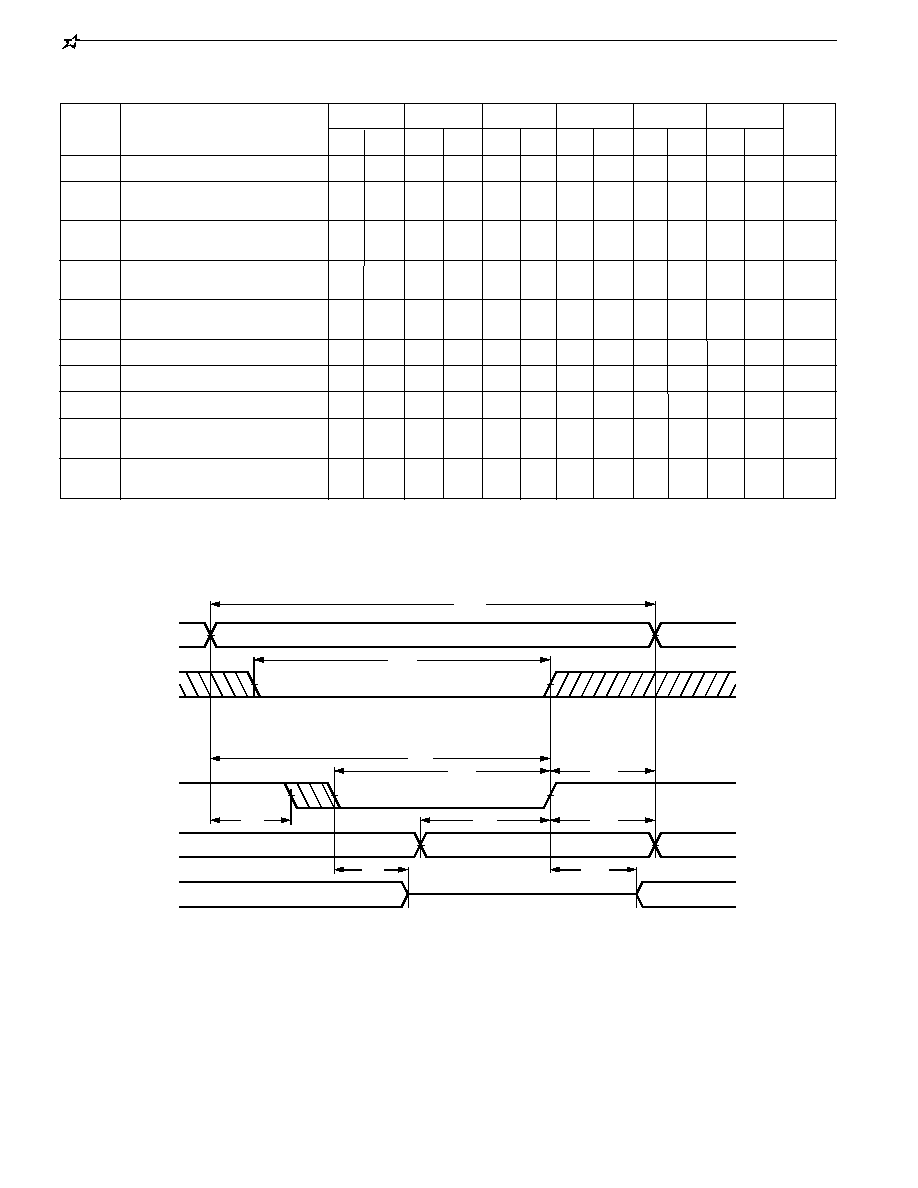
READ CYCLE NO. 2 (ADDRESS CONTROLLED)
(2)
t
ADDRESS
DATA OUT
AA
t
t
OH
DATA VALID
PREVIOUS DATA VALID
(4)
RC
READ CYCLE NO. 3 (
CE
CE
CE
CE
CE
CONTROLLED)
(2, 3)
t
CE
DATA OUT
AC
t
LZ
DATA VALID
t
PU
HIGH IMPEDANCE
(1)
(1)
t
HZ
t PUPD
t RC
(4)
VCC SUPPLY
CURRENT(5)
104
P4C174
Parameter
Symbol
Max
Max
Max
Max
Max
Max
Min
Min
Min
Min
Min
Min
t
WC
t
CW
t
AS
t
AW
Write Cycle Time
Chip Enable LOW to End of
Write
Address Valid to Beginning
of Write
Address Valid to End of
Write
t
DW
t
WP
t
AH
Data Valid to End of Write
Unit
ns
ns
ns
ns
ns
ns
≠25
≠20
≠15
≠12
≠10
≠8
End of Write to Address
Change
Write Pulse Width
End of Write to Data Change
t
DH
Write Enable HIGH to Output
LOW-Z
(1)
t
OW
Write Enable LOW to Output
HIGH-Z
(1)
t
WZ
8
7
0
7
0
7
6
0
0
4
10
9
0
9
0
9
6
0
0
4
12
10
0
10
0
10
6
0
0
AC CHARACTERISTICS - WRITE CYCLE
(V
CC
= 5V
±
10%, 0
∞
C to +70
∞
C)
4
15
12
0
12
0
12
7
0
0
5
20
15
0
15
0
15
10
0
0
7
20
15
0
15
0
15
10
0
0
7
ns
ns
ns
ns
WRITE CYCLE NO. 1 (
WE
WE
WE
WE
WE
CONTROLLED)
(6)
ADDRESS
CE
t
WC
DATA VALID
HIGH IMPEDANCE
WE
DATA IN
DATA OUT
DATA UNDEFINED
(7)
(1)
t
CW
t
AW
t
WP
t
DW
t
AH
t
DH
t
OW
t
AS
t
WZ
(1)
(8)

105
P4C174
WRITE CYCLE NO. 2 (
CE
CE
CE
CE
CE
CONTROLLED)
(6)
t
t
WE
ADDRESS
CE
DATA OUT
DATA IN
t
WC
DATA VALID
HIGH IMPEDANCE
(7)
t
AS
t
CW
t
AW
t
WP
DW
AH
t
DH
AC CHARACTERISTICS - MARCH CYCLE
(V
CC
= 5.0V
±
10%, 0
∞
C to +70
∞
C)
Parameter
Symbol
Max
Max
Max
Max
Max
Max
Min
Min
Min
Min
Min
Min
t
MC
t
ADM
t
ADMH
t
CEM
Match Cycle Time
Address Valid to MATCH
Valid
Address Change to MATCH
Change
Chip Enable LOW to
MATCH Valid
t
OEMHI
t
CEMHI
Unit
ns
ns
ns
ns
ns
ns
≠25
≠20
≠15
≠12
≠10
≠8
Chip Enable HIGH to
MATCH HIGH
Output Enable LOW to
MATCH HIGH
8
3
10
3
12
3
15
3
20
3
25
3
Data Change to MATCH
Change
t
DAMH
Data Valid to MATCH Valid
t
DAM
Write Enable LOW to
MATCH HIGH
t
WEMHI
8
10
12
15
20
25
7
8
8
10
10
15
7
8
8
10
10
15
20
15
12
10
9
7
ns
ns
ns
7
9
10
12
15
20
7
9
10
13
15
15
0
0
0
0
0
0
MATCH TIMING
ADDRESS
CE
tMC
t
OE
WE
tADM
tCEM
MATCH
VALID READ DATA OUT
DATA
VALID MATCH DATA IN
tDAM
MATCH
NO MATCH
MATCH VALID
tDAMH
tADMH
tCEMHI
tOEMHI
tWEMHI
tRMHI
RESET

106
P4C174
Mode
CE
CE
CE
CE
CE
WE
WE
WE
WE
WE
Output
Power
Standby
H
X
High Z
Standby
Read
L
H
D
OUT
Active
Write
L
L
High Z
Active
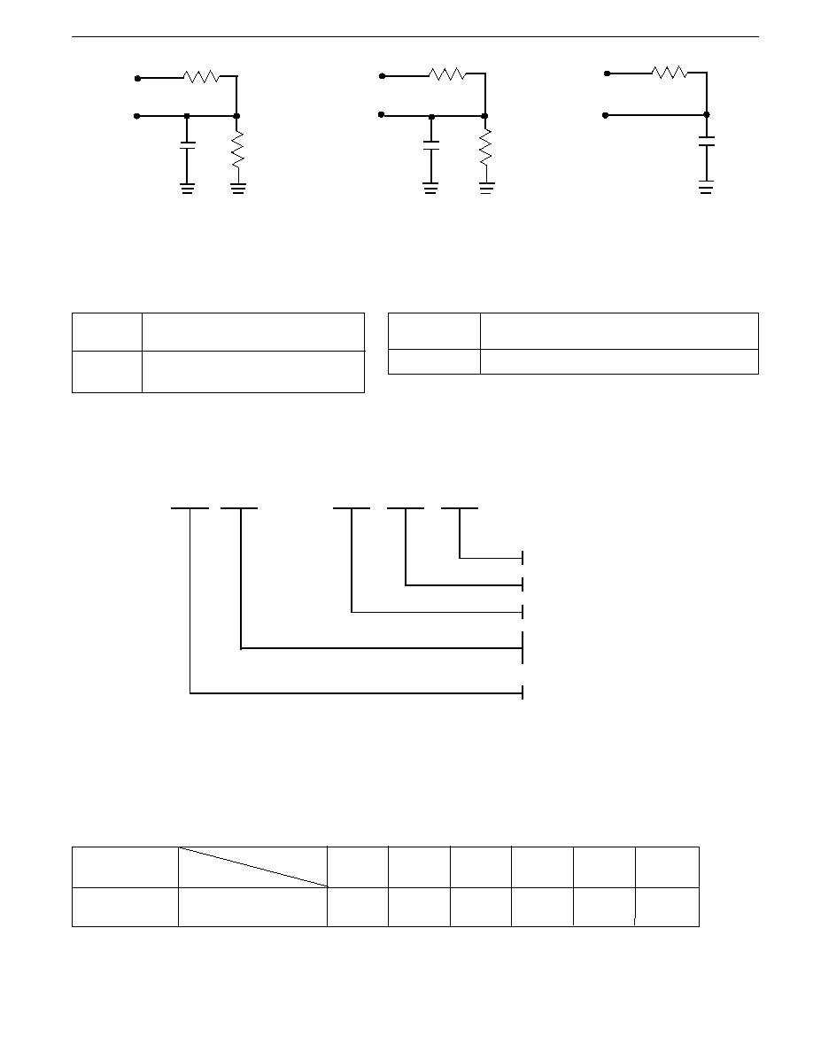
AC TEST CONDITIONS
TRUTH TABLE
RESET TIMING
t PUR
4.5 V
POWERUP
RESET
PRIOR CYCLE
INPUTS
(A, D,
CE
,
OE
,
WE
)
t RIX
NEXT CYCLE
t RPU
MATCH
t RPD
t RIR
VCC
t RMHI
t RRC
t RP
VCC SUPPLY
CURENT
AC CHARACTERISTICS - RESET CYCLE
(V
CC
= 5.0V
±
10%, 0
∞
C to +70
∞
C)
Parameter
Max
Max
Max
Max
Max
Max
Min
Min
Min
Min
Min
Min
t
RRC
t
RP
Reset Cycle Time
Reset Pulse Width
Reset LOW to Powerup
Unit
ns
ns
ns
ns
ns
≠25
≠20
≠15
≠12
≠10
≠8
35
40
45
50
50
60
t
RPU
0
Reset LOW to Powerdown
t
RPD
Reset LOW to MATCH HIGH
t
RMHI
Reset LOW to Inputs
Ignored
t
RIX
Reset LOW to inputs
Recognized
t
RIR
Powerup to RESET LOW
t
PUR
8
35
8
0
0
35
8
10
0
40
10
0
0
40
10
12
0
45
10
0
0
45
12
12
0
50
12
0
0
50
15
15
0
50
15
0
0
50
20
15
0
60
20
0
0
60
25
ns
ns
ns
Symbol
Input Pulse Levels
Input Rise and Fall Times
Input Timing Reference Level
Output Timing Reference Level
Output Load
GND to 3.0V
< 3ns
1.5V
1.5V
Outputs Loads A, B & C
107
P4C174
255
480
+5V
OUTPUT
R2
R1
INCLUDING
JIG AND
SCOPE
30 pF
OUTPUT LOAD A
+5V
R1
OUTPUT
R2
255
5 pF
INCLUDING
JIG AND
SCOPE
+5V
30 pF
MATCH
OUT
INCLUDING
JIG AND
SCOPE
R1
480
200
OUTPUT LOAD B
OUTPUT LOAD C
SELECTION GUIDE
The P4C174 is available in the following temperature, speed and package options.
Temperature
Range
Speed (ns)
Package
8
10
12
15
20
25
Commercial
Plastic DIP (300 mil)
Plastic SOJ (300 mil)
-8PC
-8JC
-10PC
-10JC
-12PC
-12JC
-15PC
-15JC
-20PC
-20JC
-25PC
-25JC
TEMPERATURE RANGE SUFFIX
Temperature
Range Suffix
C
Commercial Temp. Range, 0
∞
C to +70
∞
C.
Description
PACKAGE SUFFIX
Package
Suffix
P
Plastic DIP, 300 mil wide standard
J
Plastic SOJ, 300 mil wide standard
Description
P4C
Static RAM Prefix
174
--
ss
p
t
Temperature Range
Package Code
Speed (Access/Cycle Time)
Device Number
SS = Speed (access/cycle time in ns), e.g., 10, 12, 15
P = Package code, i.e., P, J.
T = Temperature range, i.e., C.
ORDERING INFORMATION
Performance Semiconductor's part numbering scheme is as follows:

108
P4C174