
1
P4C422
FEATURES
High Speed (Equal Access and Cycle Times)
≠ 10/12/15/20/25/35 ns (Commercial)
≠ 15/20/25 /35 ns (Military)
CMOS for Low Power
≠ 495 mW Max. ≠ 10/12/15/20/25 (Commercial)
≠ 495 mW Max. ≠ 15/20/25/35 (Military)
DESCRIPTION
The P4C422 is a 1,024-bit high-speed (10ns) Static RAM
with a 256 x 4 organization. The memory requires no
clocks or refreshing and has equal access and cycle
times. Inputs and outputs are fully TTL compatible.
Operation is from a single 5 Volt supply. Easy memory
expansion is provided by an active LOW chip select one
(
CS
1
) and active HIGH chip select two (CS
2
) as well as 3-
state outputs.
P4C422
ULTRA HIGH SPEED 256 x 4
STATIC CMOS RAM
Means Quality, Service and Speed
1Q97
FUNCTIONAL BLOCK DIAGRAM PIN CONFIGURATIONS
In addition to very high performance and very high den-
sity, the device features latch-up protection, single event
and upset protection. The P4C422 is offered in several
packages: 22-pin 400 mil DIP (plastic and ceramic), 24-
pin 300 mil SOIC, 24-pin LCC and 24-pin CERPACK.
Devices are offered in both commercial and military
temperature ranges.
COLUMN
DECODER
SENSE AMPS
32 X 32
ARRAY
CS
1
CS
2
WE
OE
O
0
O
1
O
2
O
3
A
5
A
6
A
7
A
2
A
3
A
4
A
1
A
0
D
1
D
2
D
3
D
0
DATA INPUT
CONTROL
ROW
DECODER
Single 5V
±
10% Power Supply
Separate I/O
Fully TTL Compatible Inputs and Outputs
Resistant to single event upset and latchup
resulting from advanced process and design
improvements
Standard 22-pin 400 mil DIP, 24-pin 300 mil
SOIC, 24-pin LCC package and 24-pin CERPACK
package
21
17
20
19
18
16
4
5
6
7
8
9
3
1
2
24
23
22
15
14
13
12
11
10
A1 A2 A3
A4
VCC
A
0
A5
A6
A7
GND
NC
D0
D1
D2
O1
O0
CS2
D3
O3
INDEX
WE
O2
CS1
OE
NC
1
2
3
4
5
6
7
8
9
10
11
2 2
2 1
2 0
1 9
1 8
1 7
1 6
1 5
1 4
1 3
1 2
A5
GND
A3
A2
A1
A0
A6
A7
D0
O0
D1
WE
CS2
O3
VCC
OE
D3
O2
D2
O1
A4
CS
1
1
2
3
4
5
6
7
8
9
10
11
A5
GND
A3
A2
A1
A0
A6
A7
D0
O0
D1
WE
CS2
O3
VCC
OE
D3
O2
D2
O1
A4
CS
1
12
22
21
20
19
18
17
16
15
14
13
23
24
NC
NC
SOIC (S4)
CERPACK (F3) SIMILAR
TOP VIEW
DIP (P3-1, D3-1)
TOP VIEW
LCC (L4)
TOP VIEW

2
P4C422
Grade
(2)
Ambient Temp
Gnd
Vcc
Commercial
0
∞
C to 70
∞
C
0V 5.0V
±
10%
Military
≠55
∞
C to 125
∞
C
0V 5.0V
±
10%
DC ELECTRICAL CHARACTERISTICS
Over recommended operating temperature and supply voltage
(2)
P4C422
Min
Max
V
OH
Output High Voltage
I
OH
= ≠5.2 mA, V
CC
= Min.
2.4
V
V
OL
Output Low Voltage
I
OL
= +8 mA, V
CC
= Min.
0.4
V
V
IH
Input High Voltage
2.1
V
V
IL
Input Low Voltage
0.8
V
V
CL
Input Clamp Diode Voltage
I
IN
= ≠10 mA
≠1.5
V
I
IX
Input Load Current
GND
V
IN
V
CC
≠10
10
µ
A
I
OZ
Output Current (High Z)
V
OL
V
OUT
V
OH
,
Output Disabled
≠10
10
µ
A
I
OS
Output Short Circuit
V
CC
= Max., V
OUT
= GND
90
mA
Current
(3)
Symbol
Parameter
Test Conditions
Unit
Symbol
Parameter
Conditions Typ. Unit
C
IN
Input Capacitance
V
IN
= 0V
5
pF
C
OUT
Output Capacitance V
OUT
= 0V
7
pF
CAPACITANCES
(4)
(V
CC
= 5.0V, T
A
= 25
∞
C, f = 1.0MHz)
RECOMMENDED OPERATING CONDITIONS
Symbol
Parameter
Value
Unit
T
BIAS
Temperature Under
≠ 55 to +125
∞
C
Bias
T
STG
Storage Temperature
≠ 65 to +150
∞
C
I
OUT
DC Output Current
20
mA
MAXIMUM RATINGS
(1)
Symbol
Parameter
Value
Unit
V
CC
Power Supply Pin with
≠ 0.5 to +7
V
Respect to GND
Terminal Voltage with
≠ 0.5 to
V
TERM
Respect to GND
V
CC
+0.5
V
(up to 7.0V)
T
A
Operating Temperature
≠ 55 to +125
∞
C
Notes:
1. Stresses greater than those listed under MAXIMUM RATINGS may
cause permanent damage to the device. This is a stress rating only
and functional operation of the device at these or any other conditions
above those indicated in the operational sections of this specification
is not implied. Exposure to MAXIMUM rating conditions for extended
periods may affect reliability.
2. Extended temperature operation guaranteed with 400 linear feet per
minute of air flow.
3. For test purposes, not more than one output at a time should be
shorted. Short circuit test duration should not exceed 30 seconds.
4. This parameter is sampled and not 100% tested.
5. Transition time is
3ns for 10, 12, and 15 ns products and
5ns for
20, 25, and 35 ns products, see Fig 1d. Timing is referenced at input
and output levels of 1.5V. The output loading is equivalent to the
specified I
OL
/I
OH
with a load capacitance of 15 pF (10, 12) or 30 pF
(15, 20, 25, 35) as in Fig. 1a and 1b respectively.
6. Transition time is
3ns for 10, 12, and 15 ns products and
5ns for
20, 25, and 35 ns products, see Fig 1d. Transition is measured at
steady state HIGH level -500mV or steady state LOW level +500mV
on the output from a level on the input with load shown in Fig. 1c.
7. t
W
is measured at t
WSA
= min.: t
WSA
is measured at t
W
= min.
POWER DISSIPATION CHARACTERISTICS VS. SPEED
Symbol
I
CC
Parameter
Dynamic Operating Current
Temperature
Range
Commercial
Military
-10
90
N/A
-12
90
N/A
-15
90
90
-20
90
90
-25
65
90
-35
65
90
Unit
mA
mA
3
P4C422
minimum write recovery times by eliminating the "write
recovery glitch." Reading is performed with chip selct one
(
CS
1
) LOW, chip select two (CS
2
) HIGH, write enable
(
WE
) HIGH and output enable (
OE
) LOW. The informa-
tion stored in the addressed word is read out on the
noninverting outputs (O
0
through O
3
). The outputs of the
memory go to an inactive high impedance state whenever
chip select one (
CS
1
) is HIGH, or during the write
operation when write enable (
WE
) is LOW.
An active LOW write enable (
WE
) controls the writing/
reading operation of the memory. When the chip select
one (
CS
1
) and the write enable (
WE
) are LOW and the
chip select two (CS
2
) is HIGH, the information on data
inputs (D
0
through D
3
) is written into the addressed
memory word and preconditions the output circuitry so
that true data is present at the outputs when the write
cycle is complete. This preconditioning operation insures
FUNCTIONAL DESCRIPTION
TRUTH TABLE
AC ELECTRICAL CHARACTERISTICS--READ CYCLE
(V
CC
= 5V
±
10% except as noted, All Temperature Ranges)
(2)
Mode
CS
2
CS
CS
CS
CS
CS
1
WE
WE
WE
WE
WE
OE
OE
OE
OE
OE
Output
Standby
L
X
X
X
High Z
Standby
X
H
X
X
High Z
D
OUT
Disabled
H
L
X
H
High Z
Read
H
L
H
L
D
OUT
Write
H
L
L
X
High Z
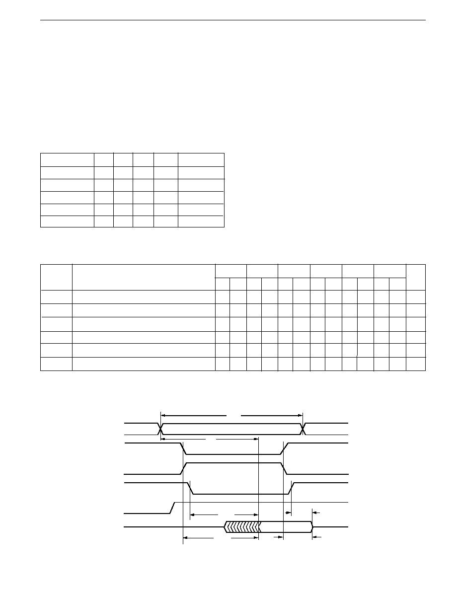
TIMING WAVEFORM OF READ CYCLE
Notes:
H = HIGH
L = Low
X = Don't Care
HIGH Z = Implies outputs are disabled or off. This
condition is defined as high impedance state
for the P4C422.
Sym.
t
RC
t
ACS
t
ZRCS
t
AOS
t
ZROS
t
AA
Read Cycle Time
(5)
Chip Select Time
(5)
Chip Select to High-Z
(6)
Output Enable Time
Output Enable to High-Z
(6)
Address Access Time
(5)
-10*
Min Max
7.5
8
7.5
8
10
-12
Min
12
Max
8
10
8
10
12
-15
Min
15
Max
8
12
8
12
15
-20
Min
20
Max
12
15
12
15
20
-25
Min
25
Max
15
20
15
20
-35
Min
35
Max
Unit
ns
ns
ns
ns
ns
ns
25
*V
CC
= 5V
±
5%
25
30
25
30
35
Parameter
12
ADDRESS
tRC
tAA
tACS
tAOS
tZROS
tZRCS
DATA VALID
CS
1
CS2
OE
WE
DATA
A0≠A7
O0≠O3
OUTPUTS

4
P4C422
Max
AC CHARACTERISTICS--WRITE CYCLE
(V
CC
= 5V
±
10% except as noted, All Temperature Ranges)
(2)
TIMING WAVEFORM OF WRITE CYCLE
Parameter
Write Cycle Time
(5)
Write Enable to High-Z
(6)
Write Recovery Time
Write Pulse Width
(5,7)
Data Setup Time Prior to Write
(5)
Data Hold Time
(5)
Address Setup Time
(5,7)
Address Hold Time
(5)
Chip Select Setup Time
(5)
Chip Select Hold Time
(5)
Sym.
t
WC
t
ZWS
t
WR
t
W
t
WSD
t
WHD
t
WSA
t
WHA
t
WSCS
t
WHCS
-10*
-12
-15
-20
-25
-35
Unit
Min Max Min Max Min Max Min
Min Max Min Max
10
8
0
2
8
8
12
9
0
10
10
15
11
0
2
12
12
20
13
2
15
15
25
15
5
20
20
35
20
5
30
25
ns
ns
ns
ns
ns
*V
CC
= 5V
±
5%
2
2
5
5
5
ns
0
0
0
2
5
5
ns
2
2
4
5
5
5
ns
0
0
0
2
5
5
ns
2
2
5
5
5
ns
tWR
tZWS
tWHCS
tWHD
tWSD
tWSA
tWSCS
tWC
CS
1
CS2
WE
ADDRESS
O0≠O3
DATA IN
D0≠D3
A0≠A7
tW
tWHA
DATA
OUTPUTS

5
P4C422
D
OUT
224
470
+5
15 pF
VTH= 1.62 V
TH
D
OUT
152
THEVENIN EQUIVALENT
D
OUT
224
470
+5
30 pF
D
OUT
224
470
+5
5 pF
Figure 1c
Figure 1d
Figure 1a
Figure 1b
AC TEST LOADS & WAVEFORMS
90%
10%
90%
10%
3.0 V
GND
Note (5)
Note (5)