
53209-580-00 C
FAS209
1
Features
s
Compliance with ANSI SCSI-2 standard
X3.131-1994 and SCSI-1
s
Compliance with ANSI X3T10/855D SCSI-3
parallel interface (SPI) standard
s
Compliance with ANSI SCSI configured
automatically (SCAM) protocol levels 1 and 2
s
Synchronous data transfers up to 10 Mbytes/sec fast
SCSI and 5 Mbytes/sec normal SCSI
s
Asynchronous data transfers up to 7 Mbytes/sec
s
Up to 12 Mbytes/sec DMA burst transfer rate
s
Clock rates up to 40 MHz
s
Supports hot plugging
s
Programmable active negation
s
Low-input capacitance
s
Programmable split-bus architecture
s
DMA interface options
s
Two bus configurations
s
On-chip, 48-mA, single-ended drivers and receivers
s
Parity pass-through on FIFO data
s
Initiator and target roles
s
SCSI sequences implemented without
microprocessor intervention
s
Part-unique ID code
s
Eight-bit, single-ended SCSI operations
Product Description
The FAS209 is a high-performance SCSI interface chip
designed to maximize transfer rates over the SCSI bus. It
is the enhanced SCSI follow-on to QLogic's FAS216 SCSI
processor chip, adding active negation and SCAM to the
FAS216 design. The FAS209 supports bidirectional,
single-ended SCSI operations. The block diagram of the
FAS209 is illustrated in figure 1.
The FAS209 maximizes transfer rates by sustaining
asynchronous data rates of up to 7 Mbytes/sec and fast,
synchronous data transfer rates of 10 Mbytes/sec. The
normal 5 Mbytes/sec synchronous transfer rate is also
supported. With its on-chip, 48-mA, single-ended drivers
and receivers, the FAS209 can connect directly to the SCSI
bus, minimizing board space requirements. The FAS209's
highly integrated structure provides users with numerous
benefits.
Initiator and target roles are supported; therefore, the
FAS209 can be used in both host adapter and peripheral
applications. The FAS209 performs such functions as bus
arbitration, selection of a target, or reselection of an
initiator. It handles message, command, status, and data
transfer between the SCSI bus and the chip's 16-byte
internal FIFO or a buffer memory. The above functions are
internal processes performed by the FAS209 chip without
microprocessor intervention.
SCAM Implementation
The FAS209 supports levels 1 and 2 of the SCAM
protocol. (Refer to the latest revision of X3T10/855D,
Annex B.) The SCAM protocol requires direct access and
control over the SCSI data bus and several of the SCSI
phase and control signals. The majority of the SCAM
protocol can be implemented in firmware at
microprocessor speeds. The following SCAM features are
supported in the hardware:
s
Arbitration without an ID
s
Slow response to selection with an unconfirmed ID
s
Detection of and response to SCAM selection
Bus Configuration
The FAS209 split-bus architecture separates the two
high-traffic information buses of the system, providing
maximum efficiency and throughput. The versatile bus
architecture supports various microprocessor and DMA
bus configurations, including those listed below:
s
Microprocessor interface via the PAD bus or the DB
bus
s
Concurrent microprocessor and DMA accesses
s
PAD bus selectable as a data-only bus
QLogic Corporation
FAS209 Fast Architecture SCSI
Data Sheet

2
FAS209
53209-580-00 C
QLogic Corporation
FAS209 bus configuration is selected by pulling the
MODE pin up or down, as shown in table 1.
Microprocessor Interface
Microprocessor interface to the FAS209 occurs over the
PAD bus or the DB bus. Both interfaces allow the
microprocessor to read and write to all the internal chip
registers, including the FIFO.
In single-bus mode (bus configuration mode 0), the
PAD bus is not used and the microprocessor must arbitrate
with other controllers for use of the DB bus. In split-bus
mode (bus configuration mode 1), the PAD bus is dedicated
to the microprocessor interface.
Pins that support the microprocessor and DMA
interfaces and other chip operations are shown in figure 2.
DMA Interface
All FAS209 DMA activity occurs over the DB bus. The
path is eight bits wide. The DB bus consists of the data
parity pin DBP0 and data pins DB7-0. Data is transferred
on DB7-0 on writes to and reads from the SCSI bus.
DACK must be active during DMA accesses. The
transfer direction is determined by the type of command
executed by the chip. DBWR strobes data into the chip.
DMA read data is driven by the chip when DACK is true.
Packaging
The FAS209 is available in a 64-pin plastic quad flat
pack (PQFP), part number 2405055; and a thin quad flat
pack (TQPF), part number 2405095. The pin diagrams are
shown in figures 2 and 4. Package dimensions are shown
in figures 3 and 5. The FAS209 pins that support
microprocessor interfaces and other chip operations are
shown in figure 6.
Table 1. Bus Modes
Mode
No.
MODE
Pin
Register
Data
DMA
Data
Configuration
0
0
DB bus
DB bus
Single bus, 8-bit
DMA
1
1
PAD bus
DB bus
Split bus, 8-bit
DMA
TRANSFER COUNT
SCSI DATA
SCSI CONTROL
DB BUS
PAD BUS
TRANSFER COUNTER
CLK CONVERSION
TEST
CONFIGURATION
SELECT/RESELECT
BUS ID
SELECT/RESELECT
TIMEOUT
SYNC OFFSET/
SYNC ASSERT/
SYNC DE-ASSERT
SYNC PERIOD
REGISTER B
US (OUT)
REGISTER B
US (IN)
COMMAND
INTERRUPT
STATUS
SEQUENCE STEP
FIFO
SEQUENCERS
Figure 1. FAS209 Block Diagram
53209-580-00 C
FAS209
5
QLogic Corporation
Electrical Characteristics
Table Notes
Conditions that exceed the operating conditions but are within the absolute maximum stress ratings may cause the
chip to malfunction.
Capacitance in and out (CIN, COUT) is 10 pF maximum for all pins, except SCSI pins.
a
Static IDD refers to all inputs at VDD, all outputs open circuit, and all bidirectional pins configured as inputs.
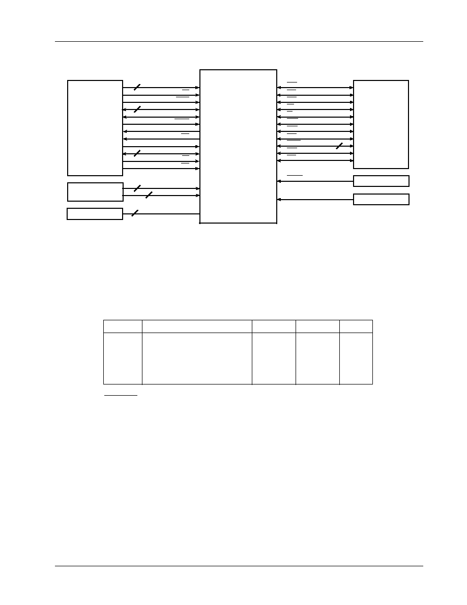
SCSI
INTERFACE
MICROPROCESSOR
AND DMA
INTERFACE
POWER AND
GROUND
A3-0
CS
DACK
DB7-0
DBP0
DBWR
DREQ
INT
MODE
PAD7-0
RD
ACK
ATN
BSY
CD
IO
MSG
SD7-0
SDP
FAS209
SEL
REQ
VDD
VSS
RESET
CLOCK
RESET
RST
CK
Figure 6. FAS209 Functional Signal Grouping
29
10
18
1
1
4
8
8
2
8
8
NO CONNECT
5
5
64
WR
Table 2. Operating Conditions
Symbol
Description
Minimum
Maximum
Unit
VDD
Supply voltage
4.75
5.25
V
IDD
a
Supply current (static IDD)
TBD
mA
IDD
Supply current (dynamic IDD)
TBD
mA
TA
Ambient temperature
0
70
o
C

