55440-580-00 A
FibreFAS440
1
Features
s
Compliant with the following Fibre Channel (FC)
technology:
Ã
Fibre Channel - Arbitrated Loop - 2 (FC-AL-2),
T11/Project 1133D/Rev 6.4
Ã
Fibre Channel - Private Loop Direct Attach
(FC-PLDA), X3T11/Project 1162DT/Rev. 2.1
Ã
Fibre Channel - Fabric Loop Attachment
(FC-FLA), T11/Project 1235-DT/Rev. 2.7
Ã
Fibre Channel - Tape (FC-TAPE), NCITS
TR-xx/Project 1315-DT/Rev. 1.07
s
Intelligent microcontroller to automate Fibre
Channel operations
s
100 Mbytes/sec data transfer rate
s
On-chip 8B/10B encode and decode
s
On-chip gigabit serial transceivers
s
16-bit DMA interface supporting transfers greater
than 100 Mbytes/sec
s
Automated command, link, and data frame
handling
s
Automated good FCP_RSP and FCP_XFER_RDY
generation
s
Data protection with buffer CRC
s
Embedded microcontroller reduces overhead in
SCSI/Fibre Channel protocol handling
s
Microprocessor interface support for Intel,
Motorola, and Hitachi (SH) processors
Product Description
The FibreFAS440 is part of the QLogic family of high
performance, low-cost, single chip, Fibre Channel
controllers. It provides external devices with high speed,
low overhead, Fibre Channel access and automated
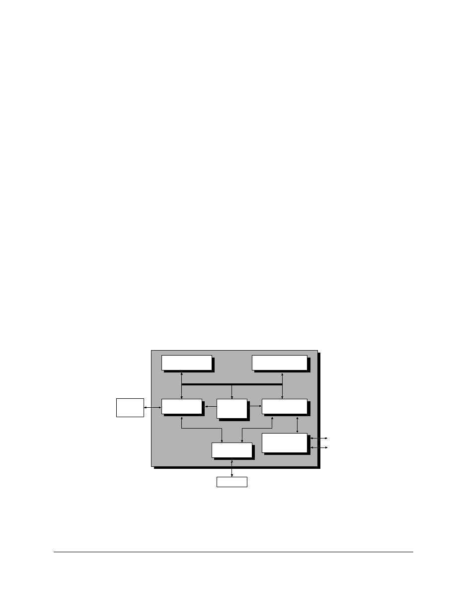
protocol handling. The FibreFAS440 block diagram is
illustrated in figure 1.
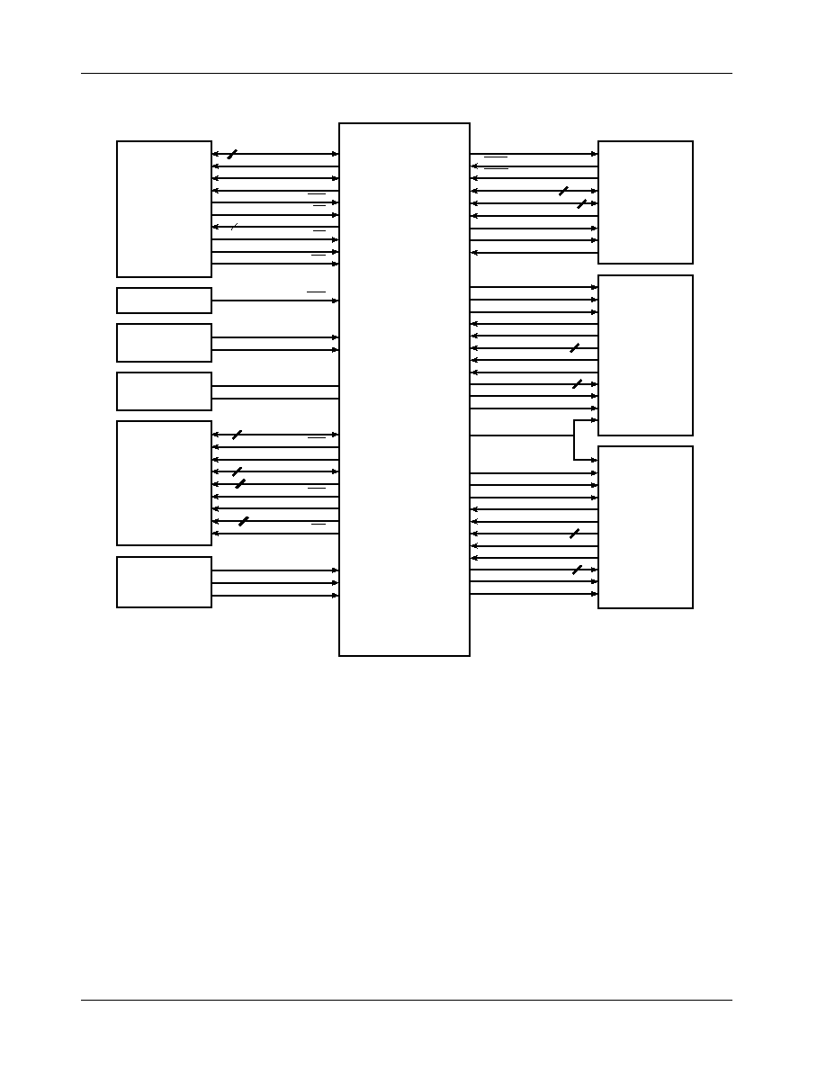
The FibreFAS440 pins that support microprocessor
interfaces and other chip operations are shown in figure 2
and described in the following paragraphs.
MICROCONTROLLER
Figure 1. FibreFAS440 Block Diagram
MICROPROCESSOR BUS
SDRAM
EXTERNAL
LOOP A
LOOP B
FibreFAS440
DMA
DEVICE
DATA
FLOW
CONTROL
BUFFER
CONTROLLER
FIBRE CHANNEL
CONTROLLER
DMA
CONTROLLER
INTERNAL
TRANSCEIVERS
MICROCONTROLLER
MICROPROCESSOR
INTERFACE LOGIC
QLogic Corporation
FibreFAS440 Dual Port Fibre Channel Controller
with Internal Transceivers
Data Sheet
2
FibreFAS440
55440-580-00 A
QLogic Corporation
Product Architecture
Fibre Channel Interface Manager
The FCIM implements the FC-AL-2 protocol,
including the FC-1 and FC-2 layers of the signaling
interface. The FC-0 layer is implemented for each port by
external serial link transmitter and receiver modules that
connect to the FCIM through two 10-bit interfaces.
The FCIM includes an 8B/10B encoder and decoder,
an elasticity buffer for clock skew management, and an
FC-AL state machine. The FCIM transmits and receives at
the full Fibre Channel rate of 106.25 Mbytes/sec.
As specified in the FC-AL protocol, the FCIM uses the
alternate buffer-to-buffer credit model to pace frames. The
FCIM receive path validates and routes frames received
from the Fibre Channel to the appropriate area in the frame
buffer. The transmit path transmits frames from the frame
buffer to the Fibre Channel. The FCIM automatically
handles frame delimiters and frame control.
The FCIM has two onboard transceivers to support
dual-loop configuration; the transceivers connect directly
to the Fibre Channel loop.
Microcontroller
The FibreFAS440 microcontroller supports the
following:
s
Maximum of 26 MIPS (50-ns instruction cycle
except for branch)
s
64 single-word instructions
s
16-bit wide instructions
Figure 2. FibreFAS440 Functional Signal Grouping
MICROPROCESSOR
INTERFACE
DBP1-0
DBOE
PAUSE
DMACLK
CKE
BA11-0
UDQM1-0
DMA
INTERFACE
BUFFER
MEMORY
INTERFACE
FibreFAS440
12
AF_AE
DB15-0
16
FF_FE
CAS
DREQ
AD15-0
ALE
16
RAS
LDQM1-0
A_LPENB
A_EN_CDET
FIBRE CHANNEL
INTERFACE
LOOP A
A_EWRAP
POR
RESET
VDD
VSS
POWER
AND GROUND
RD
WR
INT1-0
ARDY
CS
2
BHE
SIZE
ADRSEN
2
DQ31-0
32
2
SDRAMCLK
WE
VTXLO
IREF
FIBRE
CHANNEL
INTERFACE
LOGIC
TERMES
DACK
A_RCLK
A_RCLKN
A_RIN9-0
10
A_RXN
A_RXP
A_TXN
A_TXP
REFCLKO
A_TOUT9-0
10
B_LPENB
B_EN_CDET
FIBRE CHANNEL
INTERFACE
LOOP B
B_EWRAP
B_RCLK
B_RCLKN
B_RIN9-0
10
B_RXN
B_RXP
B_TXN
B_TXP
B_TOUT9-0
10
REFCLK
BC_CLK
CLOCK
2

55440-580-00 A
FibreFAS440
3
QLogic Corporation
s
Eight-bit wide data path
s
1024 instruction locations
s
32 general purpose registers
s
32 dual-port mailboxes
s
Five-level deep hardware stack
s
Direct, indirect, absolute, and immediate
addressing modes
s
Two firmware interrupt sources: I0 and I1
s
Two hardware interrupts, one with four-bit
autointerrupt vector and status
s
Full chip access through the microprocessor bus
The microcontroller allows the user to automate the
FC-AL and SCSI protocol.
The microcontroller's Harvard architecture improves
performance and flexibility by separating instruction and
data memory. Its pipelined architecture overlaps
instruction fetch and result storage with instruction decode
and execution cycles to provide two-clock instruction
execution and four-clock branch execution. The
microcontroller supports direct, indirect, absolute, and
immediate addressing modes.
The microcontroller has a 16-byte register file,
32 mailbox registers, a five-level deep stack, an integer
ALU, and other special purpose registers. The
microcontroller has access to its internal registers, the
FC-AL command FIFO, the DRAM buffer, and all registers
within the FibreFAS440. This access provides flexibility in
automating the FibreFAS440 to respond to SCSI
commands.
The microcontroller supports two types of interrupt
schemes: firmware and hardware. The firmware interrupt
allows the external microprocessor to initiate an operation
within the microcontroller without stopping the
microcontroller's current operation. The firmware interrupt
vector can be modified by the microprocessor while a
microcontroller program is running.
The hardware interrupts come directly from the Fibre
Channel module. The microcontroller can be configured to
deliver these interrupts to the microprocessor or to intercept
these interrupts and act on them as part of command
automation. Hardware interrupts handled through the
microcontroller are based on the values of the FCIM
module interrupt and status vector inputs.
Buffer Controller
The FibreFAS440 buffer controller supports the
following:
s
165 Mbytes/sec total, sustained 32-bit DMA
bandwidth
s
Data protection with 32-bit buffer CRC (BCRC)
s
Enhanced data streaming support
s
32-bit, 80 MHz synchronous DRAM (SDRAM)
support
s
Maximum buffer size of 4 Mbytes
s
High-speed buffer memory initialization and
verification to reduce power on initialization
FibreFAS440 buffer management is provided by a
multichannel, high-speed, bursting DMA controller. The
buffer controller provides the connection between the
buffer DRAM and the DMA channel, Fibre Channel, and
the microprocessor bus. The buffer controller regulates all
data movement into and out of DRAM buffer memory.
Each DMA channel supports DMA bursting, which allows
the optimal bandwidth to be maintained. Each DMA
channel has associated control, configuration, and buffer
memory address registers.
The buffer controller also provides microprocessor
address decoding, priority arbitration for the buffer
resource, BCRC, and automatic DRAM refresh control.
DMA Interface
The FibreFAS440 has a 16-bit external DMA interface
that supports burst transfer rates greater than
100 Mbytes/sec.
Microprocessor Interface
The FibreFAS440 samples the DRAM buffer address
signals during power-up reset to configure the
microprocessor operating mode. Power-down (low-power)
mode is controlled by the microprocessor.
The FibreFAS440 connects to the microprocessor as
described below:
s
Multiplexed address/data
Ã
10-bit address bus
Ã
16-bit data bus
s
Programmable byte ordering
Ã
Big endian
Ã
Little endian
s
Two interrupts
s
Support for numerous microprocessors, including:
Ã
Intel 80186, 80188, 80196
Ã
Motorola 68000, 68300, 68020, 68008
Ã
TMS 320C5X
Ã
Hitachi SH1, SH2, SH3

4
FibreFAS440
55440-580-00 A
QLogic Corporation
The following are trademark acknowledgments:
80186 and 80188 are trademarks of Intel Corporation.
68000 and 68300 series are trademarks of Motorola, Inc.
TMS is a trademark of Texas Instruments.
SH1, SH2, and SH3 are trademarks of Hitachi, Inc.
All other brand and product names are trademarks or registered trademark of their respective holders.
©October 1, 1998 QLogic Corporation, 3545 Harbor Blvd., Costa Mesa, CA 92626, (800) ON-CHIP-1 or (714) 438-2200
Specifications are subject to change without notice.
QLogic is a trademark of QLogic Corporation.