FEATURES
∑ Low current - 0.5 mA
∑ Superior CTR-2000%
∑ Superior CMR-10 kV/µs
∑ Double working voltage-480V RMS
∑ CTR guaranteed 0-70∞C
∑ U.L. recognized (File # E90700)
∑ Dual Channel - HCPL-2730
HCPL-2731
LOW INPUT CURRENT
HIGH GAIN SPLIT
DARLINGTON OPTOCOUPLERS
DESCRIPTION
The 6N138/9 and HCPL-2730/HCPL-2731 optocouplers consist of an AlGaAs LED
optically coupled to a high gain split darlington photodetector.
The split darlington configuration separating the input photodiode and the first
stage gain from the output transistor permits lower output saturation voltage and
higher speed operation than possible with conventional darlington phototransistor
optocoupler. In the dual channel devices, HCPL-2730/HCPL2731, an integrated
emitter - base resistor provides superior stability over temperature.
The combination of a very low input current of 0.5 mA and a high current transfer
ratio of 2000% makes this family particularly useful for input interface to MOS,
CMOS, LSTTL and EIA RS232C, while output compatibility is ensured to CMOS as
well as high fan-out TTL requirements.
An internal noise shield provides exceptional common mode rejection of 10 kV/µs.
An improved package allows superior insulation permitting a 480 V working voltage
compared to industry standard 220 V.
APPLICATIONS
∑ Digital logic ground isolation
∑ Telephone ring detector
∑ EIA-RS-232C line receiver
∑ High common mode noise line receiver
∑ µP bus isolation
∑ Current loop receiver
Parameter
Symbol
Value
Units
Storage Temperature
T
STG
-55 to +125
∞C
Operating Temperature
T
OPR
-40 to +85
∞C
Lead Solder Temperature
T
SOL
260 for 10 sec
∞C
EMITTER
Each Channel
I
F
(avg)
20
mA
DC/Average Forward Input Current
Peak Forward Input Current (50% duty cycle, 1 ms P.W.)
Each Channel
I
F
(pk)
40
mA
Peak Transient Input Current - (
!"
1 µs P.W., 300 pps)
I
F
(trans)
1.0
A
Reverse Input Voltage
Each Channel
V
R
5
V
Input Power Dissipation
Each Channel
P
D
35
mW
DETECTOR
Average Output Current
Each Channel
I
O
(avg)
60 mA
Emitter-Base Reverse Voltage
(6N138 and 6N139)
V
EB
0.5
V
Supply Voltage, Output Voltage
(6N138, HCPL-2730)
V
CC
, V
O
-0.5 to 7
V
(6N139, HCPL-2731)
-0.5 to 18
Output power dissipation
Each Channel
P
D
100
mW
ABSOLUTE MAXIMUM RATINGS
(No derating required up to 85∞C)
8
1
8
1
8
1
SINGLE-CHANNEL
DUAL-CHANNEL
6N138
HCPL-2730
6N139
HCPL-2731
1
2
3
4
5
6
7
8
+
_
V
F
V
CC
V
B
V
O
GND
6N138 / 6N139
N/C
N/C
1
2
3
4
5
6
7
8
+
_
V
F1
V
CC
V
01
V
02
GND
HCPL-2730 / HCPL-2731
V
F2
_
+
12/27/99 200023A

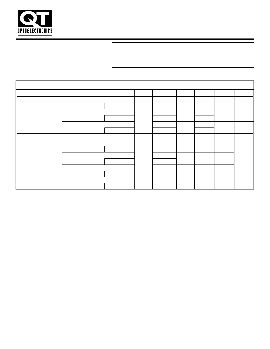
ELECTRICAL CHARACTERISTICS
(T
A
= 0 to 70∞C unless otherwise specified.)
Parameter
Test Conditions
Symbol
Device
Min
Typ**
Max
Unit
EMITTER
T
A
=25∞C)
V
F
All
1.30
1.7
V
Input Forward Voltage Each Channel (I
F
= 1.6 mA)
1.75
Input Reverse Breakdown Voltage
(T
A
= 25∞C, I
R
= 10 µA)
BV
R
All
5.0
20
V
Each Channel
Temperature coefficient of forward voltage
(I
F
= 1.6 mA)
(
#
V
F
/
#
T
A
)
All
-1.8
mV/∞C
DETECTOR
(I
F
= 0 mA, V
O
= V
CC
= 18 V)
6N139
0.01
100
µA
Logic high output current
Each Channel
I
OH
HCPL-2731
(I
F
= 0 mA, V
O
= V
CC
= 7 V)
6N138
0.01
250
Each Channel
HCPL-2730
(I
F
= 1.6 mA, V
O
= Open)
6N138
0.4
1.5
Logic low supply
(V
CC
= 18 V)
I
CCL
6N139
mA
(I
F1
= I
F2
= 1.6 mA, V
CC
= 18 V)
HCPL-2731
1.3
3
(V
O1
= V
O2
= Open, V
CC
= 7 V)
HCPL-2730
(I
F
= 0 mA, V
O
= Open)
6N138
0.05
10
Logic high supply
(V
CC
= 18 V)
I
CCH
6N139
µA
(I
F1
= I
F2
= 0 mA, V
CC
= 18 V)
HCPL-2731
0.1
20
(V
O1
= V
O2
= Open, V
CC
= 7 V)
HCPL-2730
INDIVIDUAL COMPONENT CHARACTERISTICS
SINGLE-CHANNEL
DUAL-CHANNEL
6N138
HCPL-2730
6N139
HCPL-2731
** All typicals at T
A
= 25∞C
12/27/99 200023A
LOW INPUT CURRENT
HIGH GAIN SPLIT
DARLINGTON OPTOCOUPLERS

1. Current Transfer Ratio is defined as a ratio of output collector current, I
O,
to the forward LED input current, I
F
, times 100%.
2. Pin 7 open. (6N138 and 6N139 only)
3. Common mode transient immunity in logic high level is the maximum tolerable (positive) dV
cm
/dt on the leading edge of the
common mode pulse signal, V
CM
, to assure that the output will remain in a logic high state (i.e., V
O
&
2.0 V). Common mode
transient immunity in logic low level is the maximum tolerable (negative) dV
cm
/dt on the trailing edge of the common mode pulse
signal, V
CM
, to assure that the output will remain in a logic low state (i.e., V
O
'
0.8 V).
4. Device is considered a two terminal device: Pins 1, 2, 3 and 4 are shorted together and Pins 5, 6, 7 and 8 are shorted together.
5. For dual channel devices, C
I-O
is measured by shorting pins 1 and 2 or pins 3 and 4 together and pins 5 through 8 shorted together.
6. Measured between pins 1 and 2 shorted together, and pins 3 and 4 shorted together.
NOTES
Characteristics
Test Conditions
Symbol
Min
Typ**
Max
Unit
(Relative humidity = 45%)
Input-output
(T
A
= 25∞C, t = 5 s)
I
I-O
1.0
µA
insulation leakage current
(V
I-O
= 3000 VDC)
(Note 8)
Withstand insulation test voltage
(RH
!
50%, T
A
= 25∞C)
V
ISO
2500
V
RMS
(Note 4) ( t = 1 min.)
Resistance (input to output)
(Note 4) (V
I-O
= 500 VDC)
R
I-O
10
12
$
Capacitance (input to output)
(Note 4,5) (f = 1 MHz)
C
I-O
0.6
pF
Input-Input (RH
!
45%, V
I-I
= 500 VDC) (Note 6)
I
I-I
0.005
µA
Insulation leakage current
t = 5 s, (HCPL-2730/2731 only)
Input-Input Resistance
(V
I-I
= 500 VDC) (Note 6)
R
I-I
10
11
$
(HCPL-2730/2731 only)
Input-Input Capacitance
(f = 1 MHz) (Note 6)
C
I-I
0.03
pF
(HCPL-2730/2731 only)
ISOLATION CHARACTERISTICS
(T
A
= 0 to 70∞C Unless otherwise specified)
** All typicals at T
A
= 25∞C
SINGLE-CHANNEL
DUAL-CHANNEL
6N138
HCPL-2730
6N139
HCPL-2731
12/27/99 200023A
LOW INPUT CURRENT
HIGH GAIN SPLIT
DARLINGTON OPTOCOUPLERS