 | –≠–ª–µ–∫—Ç—Ä–æ–Ω–Ω—ã–π –∫–æ–º–ø–æ–Ω–µ–Ω—Ç: HCPL-2601 | –°–∫–∞—á–∞—Ç—å:  PDF PDF  ZIP ZIP |

8
1
8
1
8
1
1
2
3
4
5
6
7
8
N/C
_
V
CC
V
E
V
O
GND
+
N/C
V
F
FEATURES
∑ Very high speed-10 MBit/s
∑ Superior CMR-10 kV/µs
∑ Double working voltage-480V
∑ Fan-out of 8 over -40∞C to +85∞C
∑ Logic gate output
∑ Strobable output
∑ Wired OR-open collector
∑ U.L. recognized (File # E90700)
DESCRIPTION
The 6N137, HCPL-2601/2611 single-channel and HCPL-2630/2631 dual-channel
optocouplers consist of a 850 nm AlGaAS LED, optically coupled to a very high
speed integrated photodetector logic gate with a strobable output. This output
features an open collector, thereby permitting wired OR outputs. The coupled
parameters are guaranteed over the temperature range of -40∞C to +85∞C. A
maximum input signal of 5 mA will provide a minimum output sink current of 13
mA (fan out of 8).
An internal noise shield provides superior common mode rejection of typically 10
kV/µs. The HCPL- 2601 and HCPL- 2631 has a minimum CMR of 5 kV/µs.
The HCPL-2611 has a minimum CMR of 10 kV/µs.
APPLICATIONS
∑ Ground loop elimination
∑ LSTTL to TTL, LSTTL or 5-volt CMOS
∑ Line receiver, data transmission
∑ Data multiplexing
∑ Switching power supplies
∑ Pulse transformer replacement
∑ Computer-peripheral interface
Input
Enable
Output
H
H
L
L
H
H
H
L
H
L
L
H
H
NC
L
L
NC
H
A 0.1 µF bypass capacitor must be connected between pins 8 and 5.
(See note 1)
TRUTH TABLE
(Positive Logic)
8/10/99 200002A
1
2
3
4
5
6
7
8
+
_
V
F1
V
CC
V
01
V
02
GND
V
F2
_
+
Dual-channel
circuit drawing
Single-channel
circuit drawing
HIGH SPEED-10 MBit/s
LOGIC GATE OPTOCOUPLERS
SINGLE-CHANNEL
DUAL-CHANNEL
6N137
HCPL-2630
HCPL-2601
HCPL-2631
HCPL-2611

RECOMMENDED OPERATING CONDITIONS
Parameter
Symbol
Min
Max
Units
Input Current, Low Level
I
FL
0
250
µA
Input Current, High Level
I
FH
*6.3
15
mA
Supply Voltage, Output
V
CC
4.5
5.5
V
Enable Voltage, Low Level
V
EL
0
0.8
V
Enable Voltage, High Level
V
EH
2.0
V
CC
V
Low Level Supply Current
T
A
-40
+85
∞C
Fan Out (TTL load)
N
8
Parameter
Symbol
Value
Units
Storage Temperature
T
STG
-55 to +125
∞C
Operating Temperature
T
OPR
-40 to +85
∞C
Lead Solder Temperature
T
SOL
260 for 10 sec
∞C
EMITTER
DC/Average Forward
Single channel
I
F
50
mA
Input Current
Dual channel (Each channel)
30
Enable Input Voltage
Single channel
V
E
5.5
V
Not to exceed V
CC
by more than 500 mV
Reverse Input Voltage
Each channel
V
R
5.0
V
Power Dissipation
Single channel
P
I
100
mW
Dual channel (Each channel)
45
DETECTOR
Supply Voltage
V
CC
7.0 V
(1 minute max)
Output Current
Single channel
I
O
50
mA
Dual channel (Each channel)
50
Output Voltage
Each channel
V
O
7.0
V
Collector Output
Single channel
P
O
85
mW
Power Dissipation
Dual channel (Each channel)
60
ABSOLUTE MAXIMUM RATINGS
(No derating required up to 85∞C)
* 6.3 mA is a guard banded value which allows for at least 20 % CTR degradation. Initial input current threshold value is 5.0 mA or less
SINGLE-CHANNEL
DUAL-CHANNEL
6N137
HCPL-2630
HCPL-2601
HCPL-2631
HCPL-2611
HIGH SPEED-10 MBit/s
LOGIC GATE OPTOCOUPLERS
8/10/99 200002A

AC Characteristics
Test Conditions
Symbol
Min
Typ**
Max
Unit
Propagation Delay Time (Note 4) (T
A
=25∞C)
T
PLH
20
45
75
ns
to Output High Level
(R
L
= 350
!
, C
L
= 15 pF) (Fig. 12)
100
Propagation Delay Time (Note 5) (T
A
=25∞C)
T
PHL
25
45
75
ns
to Output Low Level
(R
L
= 350
!
, C
L
= 15 pF) (Fig. 12)
100
Pulse Width Distortion
(R
L
= 350
!
, C
L
= 15 pF) (Fig. 12)
"
T
PHL
-T
PLH
"
3
35
ns
Output Rise Time (10-90%)
(R
L
= 350
!
, C
L
= 15 pF)
t
r
50
ns
(Note 6) (Fig. 12)
Output Fall Time (90-10%)
(R
L
= 350
!
, C
L
= 15 pF)
t
f
12
ns
(Note 7) (Fig. 12)
Enable Propagation Delay Time
(I
F
= 7.5 mA, V
EH
= 3.5 V)
t
ELH
20
ns
to Output High Level
(R
L
= 350
!
, C
L
= 15 pF) (Note 8) (Fig. 13)
Enable Propagation Delay Time
(I
F
= 7.5 mA, V
EH
= 3.5 V)
t
EHL
20
ns
to Output Low Level
(R
L
= 350
!
, C
L
= 15 pF) (Note 9) (Fig. 13)
Common Mode Transient Immunity (T
A
=25∞C)
"
V
CM
"
= 50 V, (Peak)
(at Output High Level)
(I
F
= 0 mA, V
OH
(Min.) = 2.0 V)
"
CM
H
"
V/µs
6N137, HCPL-2630
(R
L
= 350
!
) (Note 10)
10,000
HCPL-2601, HCPL-2631
(Fig. 14)
5000
10,000
HCPL-2611
"
V
CM
"
= 400 V
10,000
15,000
(R
L
= 350
!
) (I
F
= 7.5 mA, V
OL
(Max.) = 0.8 V)
10,000
Common Mode
6N137, HCPL-2630
"
V
CM
"
= 50 V (Peak)
"
CM
L
"
V/µs
Transient Immunity
HCPL-2601, HCPL-2631
(T
A
=25∞C)
5000
10,000
(at Output Low Level)
(Note 11) (Fig. 14)
HCPL-2611 (T
A
=25∞C)
"
V
CM
"
= 400 V
10,000
15,000
SWITCHING CHARACTERISTICS
(T
A
= -40∞C to +85∞C, V
CC
= 5 V, I
F
= 7.5 mA Unless otherwise specified.)
Parameter
Test Conditions
Symbol
Min
Typ**
Max
Unit
EMITTER
(I
F
= 10 mA)
V
F
1.8
V
Input Forward Voltage
T
A
=25∞C
1.4
1.75
Input Reverse Breakdown Voltage
(I
R
= 10 µA)
B
VR
5.0
V
Input Capacitance
(V
F
= 0, f = 1 MHz)
C
IN
60
pF
Input Diode Temperature Coefficient
(I
F
= 10 mA)
#
V
F
/
#
T
A
-1.4
mV/∞C
DETECTOR
7
10
High Level Supply Current
Single Channel
(V
CC
= 5.5 V, I
F
= 0 mA)
I
CCH
mA
Dual Channel
(V
E
= 0.5 V)
15
20
Low Level Supply Current
Single Channel
(V
CC
= 5.5 V, I
F
= 10 mA)
I
CCL
9
13
mA
Dual Channel
(V
E
= 0.5 V)
19
26
Low Level Enable Current
(V
CC
= 5.5 V, V
E
= 0.5 V)
I
EL
-0.8
-1.6
mA
High Level Enable Current
(V
CC
= 5.5 V, V
E
= 2.0 V)
I
EH
-0.6
-1.6
mA
High Level Enable Voltage
(V
CC
= 5.5 V, I
F
= 10 mA)
V
EH
2.0
V
Low Level Enable Voltage
(V
CC
= 5.5 V, I
F
= 10 mA) (Note 3)
V
EL
0.8
V
INDIVIDUAL COMPONENT CHARACTERISTICS
ELECTRICAL CHARACTERISTICS
(T
A
= -40∞C to +85∞C Unless otherwise specified.)
SINGLE-CHANNEL
DUAL-CHANNEL
6N137
HCPL-2630
HCPL-2601
HCPL-2631
HCPL-2611
HIGH SPEED-10 MBit/s
LOGIC GATE OPTOCOUPLERS
8/10/99 200002A

Characteristics
Test Conditions
Symbol
Min
Typ**
Max
Unit
Input-Output
(Relative humidity = 45%)
Insulation Leakage Current
(T
A
= 25∞C, t = 5 s)
I
I-O
1.0*
µA
(V
I-O
= 3000 VDC)
(Note 12)
Withstand Insulation Test Voltage
(RH < 50%, T
A
= 25∞C)
V
ISO
2500
V
RMS
(Note 12) ( t = 1 min.)
Resistance (Input to Output)
(V
I-O
= 500 V) (Note 12)
R
I-O
10
12
!
Capacitance (Input to Output)
(f = 1 MHz) (Note 12)
C
I-O
0.6
pF
ISOLATION CHARACTERISTICS
(T
A
= -40∞C to +85∞C Unless otherwise specified.)
** All typical values are at V
CC
= 5 V, T
A
= 25∞C
1.
The V
CC
supply to each optoisolator must be bypassed by a 0.1µF capacitor or larger. This can be either a ceramic or solid tantalum
capacitor with good high frequency characteristic and should be connected as close as possible to the package V
CC
and GND pins
of each device.
2.
Each channel.
3.
Enable Input - No pull up resistor required as the device has an internal pull up resistor.
4.
t
PLH
- Propagation delay is measured from the 3.75 mA level on the HIGH to LOW transition of the input current pulse to the 1.5 V
level on the LOW to HIGH transition of the output voltage pulse.
5.
t
PHL
- Propagation delay is measured from the 3.75 mA level on the LOW to HIGH transition of the input current pulse to the 1.5 V
level on the HIGH to LOW transition of the output voltage pulse.
6. t
r
- Rise time is measured from the 90% to the 10% levels on the LOW to HIGH transition of the output pulse.
7.
t
f
- Fall time is measured from the 10% to the 90% levels on the HIGH to LOW transition of the output pulse.
8.
t
ELH
- Enable input propagation delay is measured from the 1.5 V level on the HIGH to LOW transition of the input voltage pulse
to the 1.5 V level on the LOW to HIGH transition of the output voltage pulse.
9.
t
EHL
- Enable input propagation delay is measured from the 1.5 V level on the LOW to HIGH transition of the input voltage pulse
to the 1.5 V level on the HIGH to LOW transition of the output voltage pulse.
10. CM
H
- The maximum tolerable rate of rise of the common mode voltage to ensure the output will remain in the high state
(i.e., V
OUT
> 2.0 V). Measured in volts per microsecond (V/µs).
11. CM
L
- The maximum tolerable rate of rise of the common mode voltage to ensure the output will remain in the low output state
(i.e., V
OUT
< 0.8 V). Measured in volts per microsecond (V/µs).
12. Device considered a two-terminal device: Pins 1,2,3 and 4 shorted together, and Pins 5,6,7 and 8 shorted together.
NOTES
DC Characteristics
Test Conditions
Symbol
Min
Typ**
Max
Unit
High Level Output Current
(V
CC
= 5.5 V, V
O
= 5.5 V)
I
OH
100
µA
(I
F
= 250 µA, V
E
= 2.0 V) (Note 2)
Low Level Output Current
(V
CC
= 5.5 V, I
F
= 5 mA)
V
OL
.35
.06
V
(V
E
= 2.0 V, I
CL
= 13 mA) (Note 2)
Input Threshold Current
(V
CC
= 5.5 V, V
O
= 0.6 V,
I
FT
3
5
mA
V
E
= 2.0 V, I
OL
= 13 mA)
TRANSFER CHARACTERISTICS
(T
A
= -40∞C to +85∞C Unless otherwise specified.)
SINGLE-CHANNEL
DUAL-CHANNEL
6N137
HCPL-2630
HCPL-2601
HCPL-2631
HCPL-2611
HIGH SPEED-10 MBit/s
LOGIC GATE OPTOCOUPLERS
8/10/99 200002A
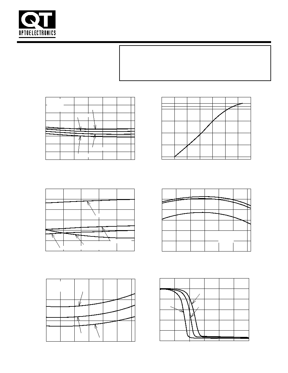
Fig.1 Low Level Output Voltage vs. Ambient Temperature
T
A
- Ambient Temperature (
∞C)
T
A
- Ambient Temperature (
∞C)
T
A
- Ambient Temperature (
∞C)
-40
-20
0
20
40
60
80
V
O
L
-Lo
w
Le
v
e
l Output
V
o
ltage (V)
0.0
0.1
0.2
0.3
0.4
0.5
0.6
0.7
0.8
I
OL
= 16 mA
I
F
- Forward Current (mA)
Fig. 4 Low Level Output Current
vs. Ambient Temperature
-40
-20
0
20
40
60
80
I
OL
-
Lo
w Le
v
e
l Output Current (mA)
20
25
30
35
40
45
50
I
F
= 5 mA
I
F
= 10 mA
I
F
= 15 mA
Fig. 5 Input Threshold Current
vs. Ambient Temperature
-40
-20
0
20
40
60
80
I
FT
- Input
Threshold Current (mA)
1
2
3
4
R
L
= 350
!
R
L
= 1k
!
R
L
= 4k
!
Fig. 6 Output Voltage vs. Input Forward Current
0
1
2
3
4
5
6
V
O
- Output
V
o
ltage (V)
0
1
2
3
4
5
6
R
L
= 350
!
R
L
= 1k
!
R
L
=4k
!
I
OL
= 6.4 mA
I
OL
= 9.6 mA
I
OL
= 12.8 mA
Conditions:
I
F
= 5 mA
V
E
= 2 V
V
CC
= 5.5V
Conditions:
V
CC
= 5.0 V
V
O
= 0.6 V
Fig. 2 Input Diode Forward Voltage
vs. Forward Current
V
F
- Forward Voltage (V)
0.9
1.0
1.1
1.2
1.3
1.4
1.5
1.6
I
F
= F
o
rw
ard Current (mA)
0.001
0.01
0.1
1
10
16
30
Conditions:
V
CC
= 5 V
V
E
= 2 V
V
OL
= 0.6 V
Fig.3 Switching Time vs. Forward Current
I
F
- Forward Current (mA)
5
7
9
11
13
15
T
P
- Propagation Dela
y
(ns)
0
20
40
60
80
100
120
V
CC
= 5 V
R
L
= 1 k
(T
PLH
)
R
L
= 4 k
!
(T
PLH
)
R
L
= 350
!
(T
PLH
)
R
L
= 1 k
!
R
L
= 4 k
!
R
L
= 350 k
!
(T
PHL
)
!$$
SINGLE-CHANNEL
DUAL-CHANNEL
6N137
HCPL-2630
HCPL-2601
HCPL-2631
HCPL-2611
HIGH SPEED-10 MBit/s
LOGIC GATE OPTOCOUPLERS
8/10/99 200002A