
© 2005 QuickLogic Corporation
www.quicklogic.com
∑
∑
∑
∑
∑
∑
1
∑ ∑ ∑ ∑ ∑ ∑
PRELIMINARY
Device Highlights
Flexible Programmable Logic
∑ 0.18 µm, six layer metal CMOS process
∑ 1.8 V core voltage, 1.8/2.5/3.3 V drive
capable I/Os
∑ Up to 202 kilobits of SRAM
∑ Up to 292 I/Os available
∑ Up to one million system gates
∑ Nonvolatile, instant-on
∑ IEEE 1149.1 boundary scan testing compliant
Embedded Dual Port SRAM
∑ Up to eight dual-port 4-kilobit high performance
SRAM blocks
∑ Embedded synchronous/asynchronous FIFO
controller
∑ Configurable and cascadable aspect ratio
Programmable I/O
∑ Bank programmable drive strength
∑ Bank programmable slew rate control
∑ Independent I/O banks capable of supporting
multiple I/O standards in one device
∑ Native support for DDR I/Os
∑ Bank programmable I/O standards: LVTTL,
LVCMOS, and LVCMOS18
Advanced Clock Network
∑ Multiple low skew clock networks
1 dedicated global clock network
4 programmable global clock networks
∑ Quadrant-based segmentable clock networks
20 quad clock networks per device
4 quad clock networks per quadrant
1 dedicated clock network per quadrant
∑ Two user Configurable Clock Managers (CCMs)
Very Low Power (VLP) Mode
∑ QuickLogic PolarPro has a special VLP pin which
can enable a low power sleep mode that
significantly reduces the overall power
consumption of the device.
∑ Enter VLP mode from normal operation in less
than 250 µs
∑ Exit from VLP mode to normal operation in less
than 250 µs
Security Links
There are several security links to disable JTAG
access to the device. Programming these optional
links completely disables access to the device from
the outside world and provides an extra level of
design security not possible in SRAM-based FPGAs.
Figure 1: QuickLogic PolarPro Block Diagram
Embedded RAM Blocks
Fabric
Embedded RAM Blocks
FIFO Controller
CCM
DDR/GPIO
GPIO
GPIO
GPIO
GPIO
GPIO
GPIO
GPIO
GPIO
GPIO
GPIO
GPIO
GPIO
DDR/GPIO
DDR/GPIO
DDR/GPIO
CCM
FIFO Controller
Combining Low Power, Performance, Density, and Embedded RAM
QuickLogic PolarProTM Data Sheet

www.quicklogic.com
© 2005 QuickLogic Corporation
∑
∑
∑
∑
∑
∑
QuickLogic PolarProTM Data Sheet Rev. A
2
PRELIMINARY
Ultra-Low Power FPGA Combining Performance, Density, and
Embedded RAM
Process Data
QuickLogic PolarPro is fabricated on a 0.18 µ, six layer metal CMOS process. The core voltage is 1.8 V. The
I/O voltage input tolerance and output drive can be set as 1.8 V, 2.5 V, and 3.3 V.
Programmable Logic Architectural Overview
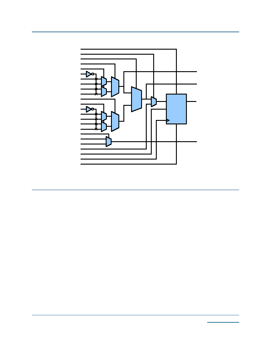
The QuickLogic PolarPro logic cell structure presented in
Figure 2
is a single register, multiplexer-based logic
cell. It is designed for wide fan-in and multiple, simultaneous output functions. The cell has a high fan-in, fits
a wide range of functions with up to 24 simultaneous inputs (including register control lines), and four outputs
(three combinatorial and one registered). The high logic capacity and fan-in of the logic cell accommodates
many user functions with a single level of logic delay.
The QuickLogic PolarPro logic cell can implement:
∑ Two independent 3-input functions
∑ Any 4-input function
∑ 8 to 1 mux function
∑ Independent 2 to 1 mux function
∑ Single dedicated register with clock enable, active high set and reset signals
∑ Direct input selection to the register, which allows combinatorial and register logic to be used separately
∑ Combinatorial logic that can also be configured as an edge-triggered master-slave D flip-flop
Table 1: PolarPro Product Family Members
Features
QL1P075
QL1P100
QL1P150
QL1P300
QL1P600
QL1P1000
Max Gates
75,000
100,000
150,000
300,000
600,000
1,000,000
Logic Cells
512
640
1,536
1,920
4,224
7,680
Max I/O
172
188
292
302
508
652
RAM Modules
8
8
12
12
22
22
FIFO Controllers
8
8
12
12
22
22
RAM bits
36,864
36,864
55,296
55,296
202,752
202,752
CCMs
2
2
2
2
2
2
Packages
TFBGA (0.8 mm)
196
196
-
-
-
-
TQFP (0.5 mm)
144
144
-
-
-
-
LBGA (1.0 mm)
256
256
256, 324
256, 324
256, 324
256, 324
© 2005 QuickLogic Corporation
www.quicklogic.com
∑
∑
∑
∑
∑
∑
QuickLogic PolarProTM Data Sheet Rev. A
3
PRELIMINARY
Figure 2: PolarPro Logic Cell
RAM Modules
The QuickLogic PolarPro family of devices includes up to eight 4-kilobit of dual-port RAM modules for
implementing RAM and FIFO functions as shown in
Figure 3
.
The RAM features include:
∑ Independently configurable read and write data bus widths
∑ Independent read and write clocks
∑ Horizontal and vertical concatenation
∑ Write byte enables
∑ Selectable pipelined or non-pipelined read data
0
0
0
0
0
0
0
0
0
1
1
1
1
1
1
1
1
1
D
E
Q
R
S
T Z
C Z
Q Z
F Z
QDS
QST
TBS
TAB
TSL
TI
TA1
TA2
TB1
TB2
BAB
BSL
BI
BA1
BA2
BB1
BB2
FS
F1
F2
QDI
QEN
QCK
QRT

www.quicklogic.com
© 2005 QuickLogic Corporation
∑
∑
∑
∑
∑
∑
QuickLogic PolarProTM Data Sheet Rev. A
4
PRELIMINARY
Figure 3: 4-Kilobit Dual-Port RAM Block
The read and write data buses of a RAM block can be arranged to variable bus widths. The bus widths can be
configured using the RAM Wizard available in QuickWorks, QuickLogic's development software. The selection
of the RAM depth and width determines how the data is addressed.
The RAM blocks also support data concatenation. Designers can cascade multiple RAM modules to increase
the depth or width by connecting corresponding address lines together and dividing the words between
modules. Generally, this requires the use of additional programmable logic resources. However, when
concatenating only two 4-kilobit RAM blocks, they can be concatenated horizontally or vertically without using
any additional programmable fabric resources.
For example, two internal dual-port RAM blocks concatenated vertically to create a 512x18 RAM block or
horizontally to create a 256x36 RAM block. A block diagram of horizontal and vertical concatenation is
displayed in
Figure 4
.
Table 2: RAM Interface Signals
Signal Name
Function
Inputs
WD [17:0]
Write Data
WA [8:0]
Write Address
WEN [1:0]
Write Enable (two 9-bit enables)
WD_SEL
Write Chip Select
WCLK
Write Clock
RA [8:0]
Read Address
RD_SEL
Read Chip Select
RCLK
Read Clock
Output
RD [17:0]
Read Data
RD[17:0]
WD[17:0]
WA[8:0]
WEN[1:0]
WD_SEL
WCLK
RA[8:0]
RD_SEL
RCLK

© 2005 QuickLogic Corporation
www.quicklogic.com
∑
∑
∑
∑
∑
∑
QuickLogic PolarProTM Data Sheet Rev. A
5
PRELIMINARY
Figure 4: Horizontal and Vertical Concatenation Examples
Table 3
shows the various RAM configurations supported by the PolarPro RAM modules.
True Dual-Port RAM
PolarPro dual-port RAM modules can also be concatenated to generate true dual-port RAMs. The true dual-
port RAM module's Port1 and Port2 have completely independent read and write ports, and separate read
and write clocks. This allows Port1 and Port2 to have different data widths and clock domains. It is important
to note that there is no circuitry preventing a write and read operation to the same address space at the same
time. Therefore, it is up to the designer to ensure that the same address is not read from and written to
simultaneously, otherwise the data is considered invalid. Likewise, the same address must not be written to
from both ports at the same time. However, it is possible to read from the same address.
Figure 5
shows an
example of a 512x18 true dual-port RAM.
Table 3: Available Dual-Port RAM Configurations
Number of RAM
Blocks
Depth
Width
1
256
1 to 18
1
512
1 to 9
2
256
1 to 36
2
512
1 to 18
2
1024
1 to 9
256x36 Dual-Port RAM
RD[35:0]
Horizontal Concatenation
512x18 Dual-Port RAM
Vertical Concatenation
WD[35:0]
WA[7:0]
WEN[3:0]
WD_SEL
WCLK
RA[7:0]
RD_SEL
RCLK
WD[17:0]
WA[8:0]
WEN[1:0]
WD_SEL
WCLK
RA[8:0]
RD_SEL
RCLK
RD[17:0]