 | –≠–ª–µ–∫—Ç—Ä–æ–Ω–Ω—ã–π –∫–æ–º–ø–æ–Ω–µ–Ω—Ç: QL3006 | –°–∫–∞—á–∞—Ç—å:  PDF PDF  ZIP ZIP |
4XLFN/RJLF &RUSRUDWLRQ
ZZZTXLFNORJLFFRP
Preliminary
'HYLFH +LJKOLJKWV
+LJK 3HUIRUPDQFH +LJK 'HQVLW\
6,000 Usable PLD Gates with 82 I/Os
300 MHz 16-bit Counters,
400 MHz Datapaths
0.35
µ
m four-layer metal non-volatile CMOS
process for smallest die sizes
(DV\WR8VH )DVW 'HYHORSPHQW
&\FOHV
100% routable with 100% utilization and
complete pin-out stability
Variable-grain logic cells provide high
performance and 100% utilization
Comprehensive design tools include high
quality Verilog/VHDL synthesis
$GYDQFHG ,2 &DSDELOLWLHV
Interfaces with both 3.3 V and 5.0 V devices
PCI compliant with 3.3 V and 5.0 V buses
for -1/-2/-3/-4 speed grades
Full JTAG boundary scan
I/O Cells with individually controlled
Registered Input Path and Output Enables
7RWDO RI ,2 SLQV
74 bidirectional input/output pins,
PCI-compliant for 5.0 V and 3.3 V buses for
-1/-2/-3/-4 speed grades
Four High Drive input-only pins
Four High Drive input-only/distributed
network pins
)RXU /RZ6NHZ 'LVWULEXWHG
1HWZRUNV
Two array clock/control networks available
to the logic cell flip-flop clock, set and reset
inputs -- each driven by an input-only pin
Two global clock/control networks available
to the logic cell; F1, clock, set and reset
inputs and the data input, I/O register clock,
reset and enable inputs as well as the output
enable control -- each driven by an input-
only or I/O pin, or any logic cell output or
I/O cell feedback
+LJK 3HUIRUPDQFH
Input + logic cell + output total delays
under 6 ns
Data path speeds over 400 MHz
Counter speeds over 300 MHz
)LJXUH S$6,& /RJLF &HOOV
4/ S$6,& )3*$ 'DWD 6KHHW
8VDEOH 3/' *DWH S$6,& )3*$ &RPELQLQJ +LJK 3HUIRUPDQFH
DQG +LJK 'HQVLW\

ZZZTXLFNORJLFFRP
4XLFN/RJLF &RUSRUDWLRQ
4/ S$6,& )3*$ 'DWD 6KHHW 5HY $
Preliminary
$UFKLWHFWXUH 2YHUYLHZ
The QL3006 is a 6,000 usable PLD gate member of the pASIC 3 family of FPGAs. pASIC 3
FPGAs are fabricated on a 0.35
µ
m four-layer metal process using QuickLogic
's patented
ViaLink
technology to provide a unique combination of high performance, high density, low
cost, and extreme ease-of-use.
The QL3006 contains 160 logic cells. With a maximum of 82 I/Os, the QL3006 is available in
68-pin PLCC, 84-pin PLCC, and 100-pin TQFP packages.
Software support for the complete pASIC 3 family, including the QL3006, is available through
three basic packages. The turnkey QuickWorks
package provides the most complete FPGA
software solution from design entry to logic synthesis, to place and route, to simulation. The
QuickTools
TM
for Workstations package provides a solution for designers who use Cadence
,
Exemplar
TM
, Mentor
, Synopsys
, Synplicity
, Viewlogic
TM
, Aldec
TM
,
or other third-party tools
for design entry, synthesis, or simulation.

4XLFN/RJLF &RUSRUDWLRQ
ZZZTXLFNORJLFFRP
4/ S$6,& )3*$ 'DWD 6KHHW 5HY $
Preliminary
(OHFWULFDO 6SHFLILFDWLRQV
$& &KDUDFWHULVWLFV DW 9
&&
9 7$
∞
& . �
To calculate delays, multiply the appropriate K factor from
7DEOH
by the numbers provided in
7DEOH
through
7DEOH
.
7DEOH /RJLF &HOOV
6\PERO
3DUDPHWHU
3URSDJDWLRQ 'HOD\V QV� )DQRXW
D
D 6WDWHG WLPLQJ IRU ZRUVW FDVH 3URSDJDWLRQ 'HOD\ RYHU SURFHVV YDULDWLRQ DW 9
&&
9 DQG
7$
∞
& 0XOWLSO\ E\ WKH DSSURSULDWH 'HOD\ )DFWRU . IRU VSHHG JUDGH YROWDJH DQG WHPSHUDWXUH
VHWWLQJV DV VSHFLILHG LQ
7DEOH
t
PD
Combinatorial Delay
b
E 7KHVH OLPLWV DUH GHULYHG IURP D UHSUHVHQWDWLYH VHOHFWLRQ RI WKH VORZHVW SDWKV WKURXJK WKH S$6,&
ORJLF FHOO LQFOXGLQJ W\SLFDO QHW GHOD\V :RUVW FDVH GHOD\ YDOXHV IRU VSHFLILF SDWKV VKRXOG EH GH
WHUPLQHG IURP WLPLQJ DQDO\VLV RI \RXU SDUWLFXODU GHVLJQ
1.4
1.7
1.9
2.2
3.2
t
SU
Setup Time
b
1.7
1.7
1.7
1.7
1.7
t
H
Hold Time
0.0
0.0
0.0
0.0
0.0
t
CLK
Clock to Q Delay
0.7
1.0
1.2
1.5
2.5
t
CWHI
Clock High Time
1.2
1.2
1.2
1.2
1.2
t
CWLO
Clock Low Time
1.2
1.2
1.2
1.2
1.2
t
SET
Set Delay
1.0
1.3
1.5
1.8
2.8
t
RESET
Reset Delay
0.8
1.1
1.3
1.6
2.6
t
SW
Set Width
1.9
1.9
1.9
1.9
1.9
t
RW
Reset Width
1.8
1.8
1.8
1.8
1.8

ZZZTXLFNORJLFFRP
4XLFN/RJLF &RUSRUDWLRQ
4/ S$6,& )3*$ 'DWD 6KHHW 5HY $
Preliminary
7DEOH ,QSXW2QO\&ORFN &HOOV
6\PERO
3DUDPHWHU
3URSDJDWLRQ 'HOD\V QV� )DQRXW
D
D 6WDWHG WLPLQJ IRU ZRUVW FDVH 3URSDJDWLRQ 'HOD\ RYHU SURFHVV YDULDWLRQ DW 9
&&
9 DQG
7$
∞
& 0XOWLSO\ E\ WKH DSSURSULDWH 'HOD\ )DFWRU . IRU VSHHG JUDGH YROWDJH DQG WHPSHUDWXUH
VHWWLQJV DV VSHFLILHG LQ
7DEOH
t
IN
High Drive Input Delay
1.5
1.6
1.8
1.9
2.4
2.9
4.4
t
INI
High Drive Input, Inverting Delay
1.6
1.7
1.9
2.0
2.5
3.0
4.5
t
ISU
Input Register Set-Up Time
3.1
3.1
3.1
3.1
3.1
3.1
3.1
t
IH
Input Register Hold Time
0.0
0.0
0.0
0.0
0.0
0.0
0.0
t
lCLK
Input Register Clock To Q
0.7
0.8
1.0
1.1
1.6
2.1
3.6
t
lRST
Input Register Reset Delay
0.6
0.7
0.9
1.0
1.5
2.0
3.5
t
lESU
Input Register clock Enable Set-Up Time
2.3
2.3
2.3
2.3
2.3
2.3
2.3
t
lEH
Input Register Clock Enable Hold Time
0.0
0.0
0.0
0.0
0.0
0.0
0.0
7DEOH &ORFN &HOOV
6\PERO
3DUDPHWHU
3URSDJDWLRQ 'HOD\V QV� /RDGV SHU +DOI &ROXPQ
D
D 7KH DUUD\ GLVWULEXWHG QHWZRUNV FRQVLVW RI KDOI FROXPQV DQG WKH JOREDO GLVWULEXWHG QHWZRUNV FRQ
VLVW RI KDOI FROXPQV HDFK GULYHQ E\ DQ LQGHSHQGHQW EXIIHU 7KH QXPEHU RI KDOI FROXPQV XVHG
GRHV QRW DIIHFW FORFN EXIIHU GHOD\ 7KH DUUD\ FORFN KDV XS WR HLJKW ORDGV SHU KDOI FROXPQ 7KH JOR
EDO FORFN KDV XS WR ORDGV SHU KDOI FROXPQ
t
ACK
Array Clock Delay
1.2
1.2
1.3
1.3
1.5
1.6
1.7
t
GCKP
Global Clock Pin Delay
0.7
0.7
0.7
0.7
0.7
0.7
0.7
t
GCKB
Global Clock Buffer Delay
0.8
0.8
0.9
0.9
1.1
1.2
1.3
7DEOH ,QSXW2QO\ ,2 &HOOV
6\PERO
3DUDPHWHU
3URSDJDWLRQ 'HOD\V QV� )DQRXW
D
t
I/O
Input Delay (bidirectional pad)
1.3
1.6
1.8
2.1
3.1
3.6
t
ISU
Input Register Set-Up Time
3.1
3.1
3.1
3.1
3.1
3.1
t
IH
Input Register Hold Time
0.0
0.0
0.0
0.0
0.0
0.0
t
lOCLK
Input Register Clock To Q
0.7
1.0
1.2
1.5
2.5
3.0
t
lORST
Input Register Reset Delay
0.6
0.9
1.1
1.4
2.4
2.9
t
lESU
Input Register clock Enable Set-Up Time
2.3
2.3
2.3
2.3
2.3
2.3
t
lEH
Input Register Clock Enable Hold Time
0.0
0.0
0.0
0.0
0.0
0.0
4XLFN/RJLF &RUSRUDWLRQ
ZZZTXLFNORJLFFRP
4/ S$6,& )3*$ 'DWD 6KHHW 5HY $
Preliminary
)LJXUH /RDGV XVHG IRU W
3;=
D 6WDWHG WLPLQJ IRU ZRUVW FDVH 3URSDJDWLRQ 'HOD\ RYHU SURFHVV YDULDWLRQ DW 9
&&
9 DQG
7$
∞
& 0XOWLSO\ E\ WKH DSSURSULDWH 'HOD\ )DFWRU . IRU VSHHG JUDGH YROWDJH DQG WHPSHUDWXUH
VHWWLQJV DV VSHFLILHG LQ
7DEOH
7DEOH 2XWSXW2QO\ ,2 &HOOV
6\PERO
3DUDPHWHU
3URSDJDWLRQ 'HOD\V QV� 2XWSXW /RDG
&DSDFLWDQFH S)�
t
OUTLH
Output Delay Low to High
2.1
2.5
3.1
3.6
4.7
t
OUTHL
Output Delay High to Low
2.2
2.6
3.2
3.7
4.8
t
PZH
Output Delay Tri-state to High
1.2
1.7
2.2
2.8
3.9
t
PZL
Output Delay Tri-state to Low
1.6
2.0
2.6
3.1
4.2
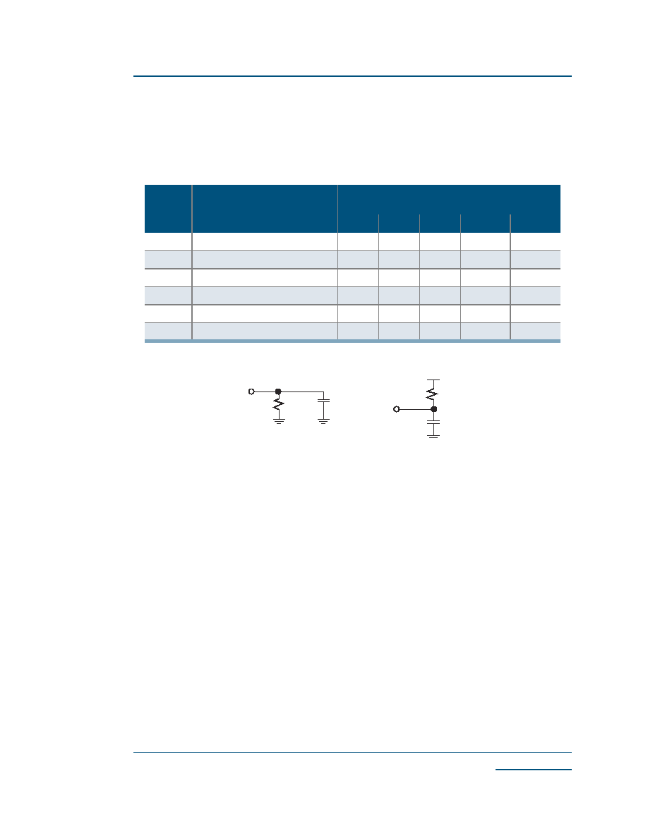
t
PHZ
Output Delay High to Tri-State
a
D 7KH ORDGV SUHVHQWHG LQ
)LJXUH
DUH XVHG IRU W
3;=
2.0
-
-
-
-
t
PLZ
Output Delay Low to Tri-State
1.2
-
-
-
-
1
1
t
PHZ
t
PLZ
5 pF
5 pF