 | –≠–ª–µ–∫—Ç—Ä–æ–Ω–Ω—ã–π –∫–æ–º–ø–æ–Ω–µ–Ω—Ç: QL5032 | –°–∫–∞—á–∞—Ç—å:  PDF PDF  ZIP ZIP |
Rev B
33 MHz/32-bit PCI Target with Embedded Programmable Logic and Dual Port SRAM
QL5130 - QuickPCI
TM
last updated 12/1099
Device Highlights
High Performance PCI Controller
s
32-bit / 33 MHz PCI Target
s
Zero-wait state PCI Target provides 132 MB/s transfer rates
s
Programmable back-end interface to optional local processor
s
Independent PCI bus (33 MHz) and local bus
(up to 160 MHz) clocks
s
Fully customizable PCI Configuration Space
s
Configurable FIFOs with depths up to 128
s
Reference design with driver code (Win 95/98/Win 2000/
NT4.0)
available
s
PCI v2.2 compliant
s
Supports Type 0 Configuration Cycles
s
3.3V, 5V Tolerant PCI signaling supports Universal PCI
Adapter designs
s
3.3V CMOS in 144-pin TQFP, 208-pin PQFP and 256-PBGA
s
Supports endian conversions
s
Unlimited/Continuous Burst Transfers Supported
Extendable PCI Functionality
s
Support for Configuration Space from 0x40 to 0x3FF
s
Multi-Function, Expanded Capabilities, & Expansion ROM
capable
s
Power management, Compact PCI, hot-swap/hot-plug
compatible
s
PCI v2.2 Power Management Spec compatible
s
PCI v2.2 Vital Product Data (VPD) configuration support
s
Programmable Interrupt Generator
s
I
2
O support with local processor
s
Mailbox register support
Programmable Logic
s
57K System gates / 619 Logic Cells
s
13,824 RAM bits, up to 157 I/O pins
s
250 MHz 16-bit counters, 275 MHz Datapaths,
160 MHz FIFOs
s
All back-end interface and glue-logic can be implemented
on chip
s
6 64-deep FIFOs (2 RAMs each) or 3 128-deep FIFOs
(4 RAMs each) or a combination that requires 12 or less
QuickLogic RAM Modules
s
(2) 32-bit busses interface between the PCI Controller and the
Programmable Logic
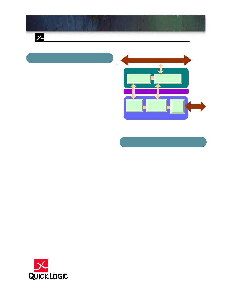
FIGURE 1. QL5130 Diagram
Architecture Overview
The QL5130 device in the QuickLogic QuickPCI ESP
(Embedded Standard Product) family provides a com-
plete and customizable PCI interface solution com-
bined with 57,000 System gates of programmable
logic. This device eliminates any need for the designer
to worry about PCI bus compliance, yet allows for the
maximum 32-bit PCI bus bandwidth (132 MB/s).
The programmable logic portion of the device con-
tains 619 QuickLogic Logic Cells, and 12 QuickLogic
Dual-Port RAM Blocks. These configurable RAM
blocks can be configured in many width/depth combi-
nations. They can also be combined with logic cells to
form FIFOs, or be initialized via Serial EEPROM on
power-up and used as ROMs. See the RAM section of
this data sheet for more information.
The QL5130 device meets PCI 2.2 electrical and tim-
ing specifications and has been fully hardware-tested.
This device also supports the Win'98 and PC'98 stan-
dards. The QL5130 device features 3.3-volt opera-
tion with multi-volt compatible I/Os. Thus it can
easily operate in 3.3-volt systems and is fully compati-
ble with 3.3V, 5V and Universal PCI card develop-
ment.
8svt
Thpr
Cvtu√Trrq
Gtvp√8ryy
$&F√Bhr
%
HC
ADAP
U6SB@U
8PIUSPGG@S
CDBC√TQ@@9
96U6√Q6UC
DIU@SA68@
QSPBS6HH67G@√√GPBD8
"!
"!
Q8D√7√±√""√HC√"!√iv√qhh√hq√hqqr
$&√Vr√DP
Q8D√8PIUSPGG@S
D
EVICE
H
IGHLIGHTS
A
RCHITECTURE
O
VERVIEW

2
Rev B
QL5130 - QuickPCI
TM
PCI Interface
The PCI target is PCI 2.2 compliant and supports
32-bit/33 MHz operation. It is capable of zero wait-
state infinite-length read and write transactions (132
MBytes/second). Transaction control is available via
the user interface as retries, wait-states, or premature
transaction termination may be induced if necessary.
The PCI configuration registers are implemented in
the programmable region of the device, leaving the
designer with ample flexibility to support optional
features.
The QL5130 device supports maximum 32-bit PCI
transfer rates, so many applications exist which are
ideally suited to the device's high performance.
High-speed data communications, telecommunica-
tions, and computing systems are just a few of the
broad range of applications areas that can benefit
from the high speed PCI interface and programmable
logic.
PCI Configuration Space
The QL5130 supports customization of required
Configuration Registers such as Vendor ID, Device
ID, Subsystem Vendor ID, etc.. QuickLogic provides
a reference Configuration Space design block.
Since the PCI Configuration Registers are imple-
mented in the programmable region of the QL5130,
the designer can implement optional features such as
multiple 32-bit Base Address Registers (BARs) and
multiple functions, as well as support the following
PCI commands: I/O Read, I/O Write, Memory Read,
Memory Write, Config Read (required), Configuration
Write (required), Memory Read Multiple, Memory
Read Line, and Memory Write and Invalidate. Addi-
tionally, the device supports Extended Capabilities
Registers, Expansion ROMs, power management,
CompactPCI hot-plug/hot-swap, Vital Product Data,
I
2
0, and mailbox registers.
PCI address and command decoding is performed by
logic in the programmable section of the device. This
allows support for any size of memory or I/O space
for back-end logic. It also allows the user to imple-
ment any subset of the PCI commands supported by
the QL5130. QuickLogic provides a reference
Address Register/Counter and Command Decode
block.
Architecture Overview
The RAM modules in the programmable region can
be used to create configurable 32-bit FIFOs. Each
32-bit FIFO can be independently assigned to Target
address space for read pre-fetch or write posting.
Using the 12 QuickLogic RAM modules, the combi-
nations include:
∑ 6 independent 64-deep FIFO (2 RAMs each),
or
∑ 3 independent 128-deep FIFOs (4 RAMs each),
or
∑ a combination of the above that requires 12 or less
QuickLogic RAM Modules
Asynchronous FIFOs (with independent read and
write clocks) are also supported.
FIGURE 2. Graphical Interface to create FIFO
PCI I
NTERFACE
A
DDRESS
AND
C
OMMAND
D
ECODE
PCI C
ONFIGURATION
S
PACE
A
RCHITECTURE
O
VERVIEW

Rev B
3
QL5130 - QuickPCI
TM
Internal PCI Interface
FIGURE 3. PCI Interface Symbol
The symbol used to connect to the PCI interface of the QL5130 is shown below. This symbol is
used in schematic or mixed schematic/HDL design flows in the QuickWorks software.
Internal PCI Interface

4
Rev B
QL5130 - QuickPCI
TM
Internal Interface Signal Descriptions
Signals used to connect to the PCI interface in the QL5130 are described below. The direction of the signal indi-
cates if it is an input provided by the local interface (I) or an output provided by the PCI interface (O).
Usr_Addr_WrData[31:0]
O
Target address, and data from target writes. During all target
accesses, the address will be presented on
Usr_Addr_WrData[31:0] and simultaneously, Usr_Adr_Valid will
be active. During target write transactions, this port will also
present write data to the PCI configuration space or user logic.
Usr_CBE[3:0]
O
PCI command and byte enables. During target accesses, the PCI
command will be presented on Usr_CBE[3:0] and simultaneously,
Usr_Adr_Valid will be active. During target read or write
transactions, this port will present active-low byte-enables to the
PCI configuration space or user logic.
Usr_Adr_Valid
O
Indicates the beginning of a PCI transaction, and that a target
address is valid on Usr_Addr_WrData[31:0] and the PCI
command is valid on Usr_CBE[3:0]. When this signal is active,
the target address must be latched and decoded to determine if this
address belongs to the device's memory space. Also, the PCI
command must be decoded to determine the type of PCI
transaction. On subsequent clocks of a target access, this signal
will be low, indicating that an address is NOT present on
Usr_Addr_WrData[31:0].
Usr_Adr_Inc
O
Indicates that the target address should be incremented, because
the previous data transfer has completed. During burst target
accesses, the target address is only presented to the back-end logic
at the beginning of the transaction (when Usr_Adr_Valid is
active), and must therefore be latched and incremented (by 4) for
subsequent data transfers. Note that during write transactions,
Usr_Adr_Inc indicates valid data on Usr_Addr_WrData[31:0] that
must be accepted by the back-end logic (regardless of the state of
Usr_Rdy). During read transactions, Usr_Adr_Inc will signal to
the back-end that the PCI core is ready to accept data.
Usr_Adr_Inc and Usr_Rdy both active during a read transaction
signals a data transfer between the FPGA and the PCI core (and
that the address counter must be incremented).
Usr_RdDecode
I
This signal should be driven active when a "user read" command
has been decoded from the Usr_CBE[3:0] bus (while
Usr_Adr_Valid is active). This command may be mapped from
any of the PCI "read" commands, such as Memory Read, Memory
Read Line, Memory Read Multiple, I/O Read, etc.
Usr_WrDecode
I
This signal should be driven active when a "user write" command
has been decoded from the Usr_CBE[3:0] bus (while
Usr_Adr_Valid is active). This command may be mapped from
any of the PCI "write" commands, such as Memory Write or I/O
Write.
Internal Interface
Signal Descriptions

Rev B
5
QL5130 - QuickPCI
TM
Internal Interface Signal Descriptions (Continued)
Usr_Select
I
This signal should be driven active when the address on
Usr_Addr_WrData[31:0] has been decoded and determined to be
within the address space of the device. Usr_Addr_WrData[31:0]
must be compared to each of the valid Base Address Registers in
the PCI configuration space. Also, this signal must be gated by the
Memory Access Enable or I/O Access Enable registers in the PCI
configuration space (Command Register bits 1 or 0 at offset 04h).
Usr_Write
O
This signal will be active throughout a "user write" transaction,
which has been decoded by Usr_WrDecode at the beginning of the
transaction. The write-enable for individual double-words of data
(on Usr_Addr_WrData[31:0]) during a user write transaction
should be generated by logically ANDing this signal with
Usr_Adr_Inc.
Cfg_Write
O
This signal will be active throughout a configuration write
transaction. The write-enable for individual double-words of data
(on Usr_Addr_WrData[31:0]) during a configuration write
transaction should be generated by logically ANDing this signal
with Usr_Adr_Inc.
Cfg_RdData[31:0]
I
Data from the PCI configuration registers, required to be presented
to the PCI core during PCI configuration reads.
Usr_RdData[31:0]
I
Data from the back-end user logic, required to be presented during
PCI reads.
Cfg_CmdReg8
Cfg_CmdReg6
I
Bits 6 and 8 from the Command Register in the PCI configuration
space (offset 04h).
Cfg_PERR_Det
O
Parity error detected on the PCI bus. When this signal is active, bit
15 of the Status Register must be set in the PCI configuration
space (offset 04h).
Cfg_SERR_Sig
O
System error asserted on the PCI bus. When this signal is active,
the Signaled System Error bit, bit 14 of the Status Register, must
be set in the PCI configuration space (offset 04h).
Usr_TRDYN
O
Copy of the TRDYN signal as driven by the PCI target interface.
Usr_STOPN
O
Copy of the STOPN signal as driven by the PCI target interface.
Usr_Devsel
O
Inverted copy of the DEVSELN signal as driven by the PCI target
interface.
Usr_Last_Cycle_D1
O
Indicates that the last transfer in a PCI transaction is occurring.
RdPipe_Stat[1:0]
O
Indicates the number of dwords currently in the read pipeline
("00" = 0 elements, "01" = 1 element, "11" = 2 elements). This
value is important at the end of a transaction (i.e. when
Usr_Last_Cycle_D1 is active) if non-prefetchable memory is
being read. Non-prefetchable memory is defined as registers or
memory elements whose value changes when they are read.
Examples are status registers which are cleared when they are
read, or FIFO memories, since consecutive reads from the same
address in these elements may not produce the same data values.
Usr_Rdy
I
Used to delay (add wait states to) a PCI transaction when the back
end needs additional time. Subject to PCI latency restrictions.
Usr_Stop
I
Used to prematurely stop a PCI target access on the next PCI
clock.