 | –≠–ª–µ–∫—Ç—Ä–æ–Ω–Ω—ã–π –∫–æ–º–ø–æ–Ω–µ–Ω—Ç: QL5732 | –°–∫–∞—á–∞—Ç—å:  PDF PDF  ZIP ZIP |

© 2003 QuickLogic Corporation
www.quicklogic.com
∑
∑
∑
∑
∑
∑
1
∑ ∑ ∑ ∑ ∑ ∑
Device Highlights
High Performance PCI Controller
∑
32-bit/33 MHz PCI Master/Target
∑
Zero-wait state PCI Master provides
132 MBps transfer rates
∑
Zero-wait-state PCI Target Write/One-wait-state
PCI Target Read interface
∑
Supports all PCI commands, including
configuration and MWI
∑
Supports fully-customizable byte enable for
master channels
∑
Target interface supports retry, disconnect
with/without data transfer, and target abort
∑
Fully programmable back-end interface
∑
Independent PCI bus (33 MHz) and local bus (up
to 160 MHz) clocks
∑
Fully customizable PCI Configuration Space
∑
Configurable FIFOs with depths up to 256 words
∑
Reference design with driver code (Win
95/98/Win 2000/NT4.0) available
∑
PCI v2.3 compliant
∑
Supports Type 0 Configuration Cycles in Target
mode
∑
3.3 V PCI signaling
∑
2.5 V Supply Voltage
∑
484 and 280-pin PBGA
∑
Supports Extendable PCI functionality
∑
Unlimited/Continuous Burst Transfers supported
Extendable PCI Functionality
∑
Support for PCI host-bridge function
∑
Support for Configuration Space from
0
◊ 40 to 0 ◊ 3FF
∑
Multi-Function, Expanded Capabilities, and
Expansion ROM capable
∑
PCI v2.3 Power Management Spec compatible
∑
PCI v2.3 Vital Product Data (VPD) configuration
support
∑
Programmable Interrupt Generator
∑
I
2
O support with local processor
∑
Mailbox register support
Flexible Programmable Logic
∑
1,348 Logic Cells
∑
50,688 RAM bits
∑
Up to 262 I/O pins
∑
All back-end interface and glue-logic can be
implemented on chip
∑
Six 32-bit busses interface between the PCI
Controller and the Programmable Logic
∑
Twenty-two 2,304 bit Dual Port High
Performance SRAM Blocks
∑
3,482 flip-flops available
Figure 1: 5732 Block Diagram
PCI Bus
PCI Bus 33 MHz/32 bits (data and
address)
Target
Controller
160 MHz
FIFOs
Config
space
DMA
Controller
Master
Controller
High Speed
Logic Cells
High
Speed
Data
Path
Programmable
Logic
32 bit Interface
264 User I/O
QL5732 Enhanced QuickPCI
Device Data Sheet
33 MHz/32-bit PCI Master/Target with Embedded Programmable Logic and
Dual Port SRAM

www.quicklogic.com
© 2003 QuickLogic Corporation
∑
∑
∑
∑
∑
∑
QL5732 Enhanced QuickPCI Device Data Sheet Rev D
2
Architecture Overview
The QL5732 device in the QuickLogic
QuickPCI Embedded Standard Product (ESP) family
provides a complete and customizable PCI interface solution combined with programmable logic.
This device eliminates any need for the designer to worry about PCI bus compliance, yet allows
for the maximum 32-bit PCI bus bandwidth (132 MBps).
The programmable logic portion of the device contains 1,348 QuickLogic Logic Cells and
22 QuickLogic Dual-Port RAM Blocks. These configurable RAM blocks can be configured in
many width/depth combinations. They can also be combined with logic cells to form FIFOs, or
be initialized via Serial EEPROM on power-up and used as ROMs.
The QL5732 device meets PCI 2.3 electrical and timing specifications and has been fully
hardware-tested. This device also supports the Win'98 and PC'98 standards. The QL5732 device
features 2.5 V operation with multi-volt compatible I/Os. The device can easily operate in 3 V
embedded systems and is fully compatible with 3.3 V applications.
PCI Controller
The PCI Controller is a 32-bit/33 MHz PCI 2.3 Compliant Master/Target Controller capable of
infinite length Master Write and Read transactions at zero wait states (132 MBps).
The Master will never insert wait states during transfers, so data is supplied or received by FIFOs
that can be configured in the programmable region of the device. The Master is capable of
initiating any type of PCI commands, including configuration cycles and Memory Write and
Invalidate (MWI). This enables the QL5732 device to act as a PCI host. The Master Controller will
most often be operated by a DMA Controller in the programmable region of the device. DMA
Controller reference design is available and will be included in the QuickWorks
design software.
The Target interface offers full PCI Configuration Space and flexible target addressing. It supports
zero-wait-state target Write and one-wait-state target Read operations. It also supports retry,
disconnect with/without data transfer, and target abort requested by the back end. Any number
of 32-bit BARs may be configured as either memory or I/O space. All required and optional
PCI 2.3 Configuration Space registers can be implemented within the programmable region of
the device. A reference design of a Target Configuration and Addressing module is available and
will be included in the QuickWorks design software.
The interface ports are divided into a set of ports for master transactions and a set for target
transactions. The Master DMA controller and Target Configuration Space and Address Decoding
are done in the programmable logic region of the device. These functions are not timing critical,
so leaving these elements in the programmable region allows the greatest degree of flexibility to
the designer. Reference DMA controller, Configuration Space, and Address Decoding blocks are
readily available so that the design cycle can be minimized.

© 2003 QuickLogic Corporation
www.quicklogic.com
∑
∑
∑
∑
∑
∑
QL5732 Enhanced QuickPCI Device Data Sheet Rev D
3
Configuration Space and Address Decode
The configuration space is completely customizable in the programmable region of the device.
PCI address and command decoding is performed by logic in the programmable section of the
device. This allows support for any size of memory or I/O space for back end logic. It also allows
the user to implement any subset of the PCI commands supported by the QL5732. QuickLogic
provides a reference Address Register/Counter and Command Decode block.
DMA Master Target Controller
The customizable DMA controller included with the QuickWorks design software contains the
following features:
∑
Configurable DMA count size for Reads and Writes (up to 30-bits)
∑
Configurable DMA burst size for PCI (including unlimited/continuous burst)
∑
Customizable PCI command to use by core
∑
Customizable Byte Enable signal
∑
Programmable Arbitration between DMA Read & Write transactions
∑
DMA Registers may be mapped to any area of Target Memory Space, including:
∑
Read Address (32-bit register)
∑
Write Address (32-bit register)
∑
Read Length (16-bit register) / Write Length (16-bit register)
∑
Control and Status (32-bit register, includes 8 bit Burst Length)
∑
DMA Registers are available to the local design or the PCI bus
∑
Programmable Interrupt Control to signal end of transfer or other event

www.quicklogic.com
© 2003 QuickLogic Corporation
∑
∑
∑
∑
∑
∑
QL5732 Enhanced QuickPCI Device Data Sheet Rev D
4
Configurable FIFOs
FIFOs may be created with the RAM/FIFO wizard in the QuickWorks tools.
Figure 2
shows the
graphical interface used to create these FIFOs. FIFOs may be designed up to
1,024 words deep. The 22 RAM cells available in the QL5732 allow for up to:
∑
11 FIFOs at 128 words deep (36 wide)
∑
5 FIFOs at 256 words deep (36 wide)
∑
2 FIFOs at 512 words deep (44 wide)
∑
1 FIFO at 1,024 words deep (44 wide)
Figure 2: Graphical Interface to create FIFO
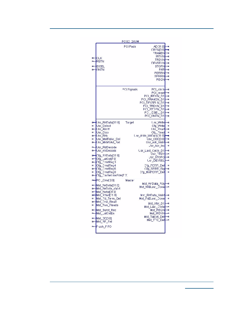
PCI Interface Symbol
Figure 2
shows the graphical interface symbol numbers you have to use in your schematic design
in order to attach the local interface programmable logic design to the PCI core. If you are
designing with a top-level Verilog or VHDL file you must use a structural instantiation of this
PCI32_25µm block (
Figure 3
) instead of a graphical symbol.
© 2003 QuickLogic Corporation
www.quicklogic.com
∑
∑
∑
∑
∑
∑
QL5732 Enhanced QuickPCI Device Data Sheet Rev D
5
Figure 3: PCI Interface Symbol