
© 2002 QuickLogic Corporation
www.quicklogic.com
1
∑
∑
∑
∑
∑
∑
∑ ∑ ∑ ∑ ∑ ∑
Device Highlights
Flexible Programmable Logic
∑
.25
µ
m, Five layer metal CMOS Process
∑
2.5 V V
CC
, 2.5 V/3.3 V Drive Capable I/O
∑
3,032 Logic Cells
∑
488,064 Max System Gates
∑
Up to 444 I/O Pins
Embedded Dual Port SRAM
∑
Thirty six 2,304-bit Dual Port High
Performance SRAM Blocks
∑
82,900 RAM Bits
∑
RAM/ROM/FIFO Wizard for Automatic
Configuration
∑
Configurable and Cascadable
Programmable I/O
∑
High performance Enhanced I/O (EIO):
Less than 3 ns Tco
∑
Programmable Slew Rate Control
∑
Programmable I/O Standards:
∑
LVTTL, LVCMOS, PCI, GTL+, SSTL2,
and SSTL3
∑
Eight Independent I/O Banks
∑
Three Register Configurations: Input,
Output, and Output Enable
Advanced Clock Network
∑
Nine Global Clock Networks:
∑
One Dedicated
∑
Eight Programmable
∑
20 Quad-Net Networks: Five per Quadrant
∑
16 I/O Controls: Two per I/O Bank
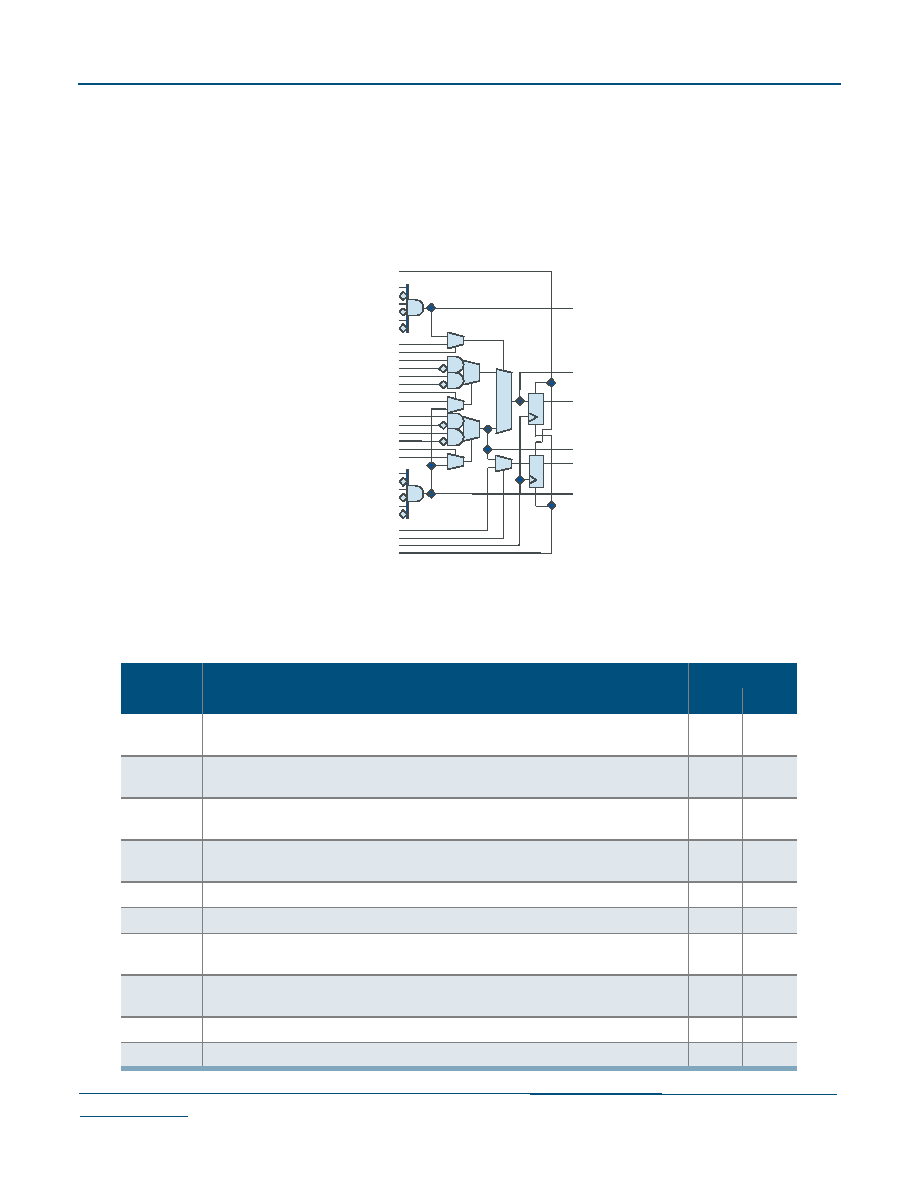
Figure 1: Eclipse Block Diagram
Memory - Dual Port RAM
High Speed Logic Cells
488K Gates
Memory - Dual Port RAM
Combining Performance, Density and Embedded RAM
QL6500 Eclipse Data Sheet
2
www.quicklogic.com
© 2002 QuickLogic Corporation
∑
∑
∑
∑
∑
∑
QL6500 Eclipse Data Sheet Rev C
Electrical Specifications
AC Characteristics at V
CC
= 2.5 V, TA = 25∞ C (K = 0.74)
The AC Specifications are provided from
Table 1
to
Table 10
. Logic Cell diagrams and
waveforms are provided from
Figure 2
to
Figure 15
.
Figure 2: Eclipse Logic Cell
Table 1: Logic Cells
Symbol
Parameter
Value (ns)
Logic Cells
Min
Max
t
PD
Combinatorial Delay of the longest path: time taken by the combinatorial circuit to
output
-
0.257
t
SU
Setup time: time the synchronous input of the flip-flop must be stable before the
active clock edge
0.22
-
t
HL
Hold time: time the synchronous input of the flip-flop must be stable after the active
clock edge
0
-
t
CO
Clock to out delay: the amount of time taken by the flip-flop to output after the
active clock edge.
-
0.255
t
CWHI
Clock High Time: required minimum time the clock stays high
0.46
-
t
CWLO
Clock Low Time: required minimum time that the clock stays low
0.46
-
t
SET
Set Delay: time between when the flip-flop is "set" (high)
and when the output is consequently "set" (high)
-
0.18
t
RESET
Reset Delay: time between when the flip-flop is "reset" (low) and when the output
is consequently "reset" (low)
-
0.09
t
SW
Set Width: time that the SET signal remains high/low
0.3
-
t
RW
Reset Width: time that the RESET signal remains high/low
0.3
-
© 2002 QuickLogic Corporation
www.quicklogic.com
3
∑
∑
∑
∑
∑
∑
QL6500 Eclipse Data Sheet Rev C
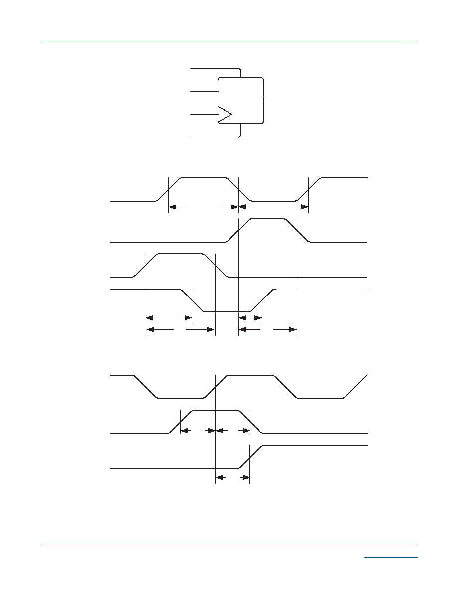
Figure 3: Logic Cell Flip Flop
Figure 4: Logic Cell Flip Flop Timings - First Waveform
Figure 5: Logic Cell Flip Flop Timings - Second Waveform
SET
D
CLK
RESET
Q
SET
RESET
Q
CLK
t
CWHI
(min)
t
CWLO
(min)
t
RESET
t
RW
t
SET
t
SW
CLK
D
Q
t
SU
t
HL
t
CO

4
www.quicklogic.com
© 2002 QuickLogic Corporation
∑
∑
∑
∑
∑
∑
QL6500 Eclipse Data Sheet Rev C
Figure 6: Eclipse Global Clock Structure
Figure 7: Global Clock Structure Schematic
Table 2: Eclipse Clock Performance
Clock
Parameters
Clock Performance
Global
Dedicated
Logic Cells (Internal)
Clock signal generated internally
1.51 ns (max)
1.59 ns (max)
I/O's (External)
Clock signal generated externally
2.06 ns (max)
1.73 ns (max)
Table 3: Eclipse Global Clock Performance
Clock Segment
Parameter
Value (ns)
Min
Max
t
PGCK
Global clock pin delay to quad net
-
1.34
t
BGCK
Global clock buffer delay
(quad net to flip flop)
-
0.56
Quad net
Programmable Clock
External Clock
Global Clock Buffer
Global Clock
t
PGCK
t
BGCK
Clock
Select
© 2002 QuickLogic Corporation
www.quicklogic.com
5
∑
∑
∑
∑
∑
∑
QL6500 Eclipse Data Sheet Rev C
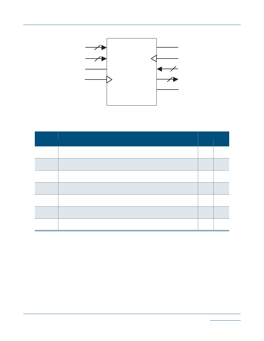
Figure 8: RAM Module
Table 4: RAM Cell Synchronous Write Timing
Symbol
Parameter
Value (ns)
RAM Cell Synchronous Write Timing
Min
Max
t
SWA
WA setup time to WCLK: time the WRITE ADDRESS must be stable before the
active edge of the WRITE CLOCK
0.675
-
t
HWA
WA hold time to WCLK: time the WRITE ADDRESS must be stable after the active
edge of the WRITE CLOCK
0
-
t
SWD
WD setup time to WCLK: time the WRITE DATA must be stable before the active
edge of the WRITE CLOCK
0.654
-
t
HWD
WD hold time to WCLK: time the WRITE DATA must be stable after the active edge
of the WRITE CLOCK
0
-
t
SWE
WE setup time to WCLK: time the WRITE ENABLE must be stable before the active
edge of the WRITE CLOCK
0.623
-
t
HWE
WE hold time to WCLK: time the WRITE ENABLE must be stable after the active
edge of the WRITE CLOCK
0
-
t
WCRD
WCLK to RD (WA = RA): time between the active WRITE CLOCK edge and the
time when the data is available at RD
-
4.38
WA
WD
WE
WCLK
RE
RCLK
RA
RD
RAM Module
[9:0]
[17:0]
[9:0]
[17:0]
ASYNCRD