
∑ ∑ ∑ ∑ ∑ ∑
© 2003 QuickLogic Corporation
www.quicklogic.com
∑
∑
∑
∑
∑
∑
1
Device Highlights
Flexible Programmable Logic
∑
0.25
µ
m five layer metal CMOS Process
∑
2.5 V V
CC
, 2.5 V/3.3 V Drive Capable I/O
∑
1,536 Logic Cells
∑
320,640 Max System Gates
∑
Up to 310 I/O Pins
Embedded Dual Port SRAM
∑
Twenty-four 2,304-bit Dual Port High
Performance SRAM Blocks
∑
55,300 RAM bits
∑
RAM/ROM/FIFO Wizard for Automatic
Configuration
∑
Configurable and Cascadable
Programmable I/O
∑
High performance Enhanced I/O (EIO)--
less than 3 ns Tco
∑
Programmable Slew Rate Control
∑
Programmable I/O Standards:
∑
LVTTL, LVCMOS, PCI, GTL+, SSTL2,
and SSTL3
∑
Eight Independent I/O Banks
∑
Three Register Configurations: Input,
Output, and Output Enable
Advanced Clock Network
∑
Nine Global Clock Networks:
∑
One Dedicated
∑
Eight Programmable
∑
20 Quad-Net Networks--five per Quadrant
∑
16 I/O Controls--two per I/O Bank
∑
Four phase locked loops
Embedded Computational Units
ECUs provide integrated Multiply, Add, and
Accumulate Functions.
Figure 1: EclipsePlus Block Diagram
Memory - Dual Port RAM
Memory - Dual Port RAM
PLL
PLL
PLL
PLL
Embedded Computational Units
High Speed Logic Cells
321K Gates
Combining Performance, Density, and Embedded RAM
QL7120 EclipsePlus Data Sheet
www.quicklogic.com
© 2003 QuickLogic Corporation
∑
∑
∑
∑
∑
∑
QL7120 EclipsePlus Data Sheet Rev C
2
Electrical Specifications
AC Characteristics*
*(at V
CC
= 2.5 V, TA = 25∞ C, Typical Corner, Speed Grade = -7 (K = 1.00))
The AC Specifications are provided from
Table 1
to
Table 9
. Logic Cell diagrams and
waveforms are provided from
Figure 2
to
Figure 15
.
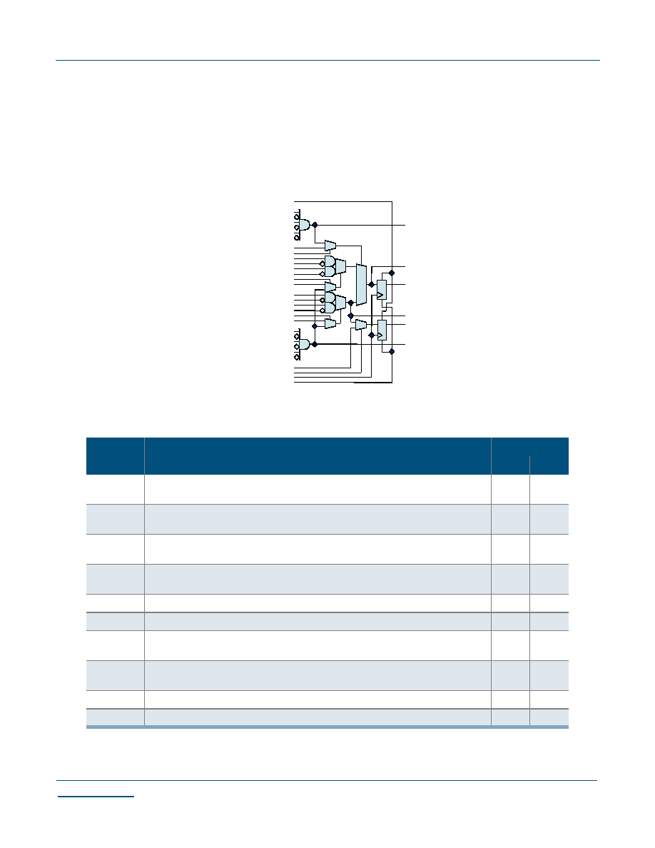
Figure 2: EclipsePlus Logic Cell
Table 1: Logic Cells
Symbol
Parameter
Value (ns)
Logic Cells
Min
Max
t
PD
Combinatorial Delay of the longest path: time taken by the combinatorial circuit to
output
0.205
1.01
t
SU
Setup time: time the synchronous input of the flip flop must be stable before the
active clock edge
0.231
-
t
HL
Hold time: time the synchronous input of the flip flop must be stable after the active
clock edge
0
-
t
CO
Clock to out delay: the amount of time taken by the flip flop to output after the
active clock edge.
-
0.427
t
CWHI
Clock High Time: required minimum time the clock stays high
0.46
-
t
CWLO
Clock Low Time: required minimum time that the clock stays low
0.46
-
t
SET
Set Delay: time between when the flip flop is "set" (high)
and when the output is consequently "set" (high)
-
0.585
t
RESET
Reset Delay: time between when the flip flop is "reset" (low) and when the output
is consequently "reset" (low)
-
0.658
t
SW
Set Width: time that the SET signal remains high/low
0.3
-
t
RW
Reset Width: time that the RESET signal remains high/low
0.3
-

© 2003 QuickLogic Corporation
www.quicklogic.com
∑
∑
∑
∑
∑
∑
QL7120 EclipsePlus Data Sheet Rev C
3
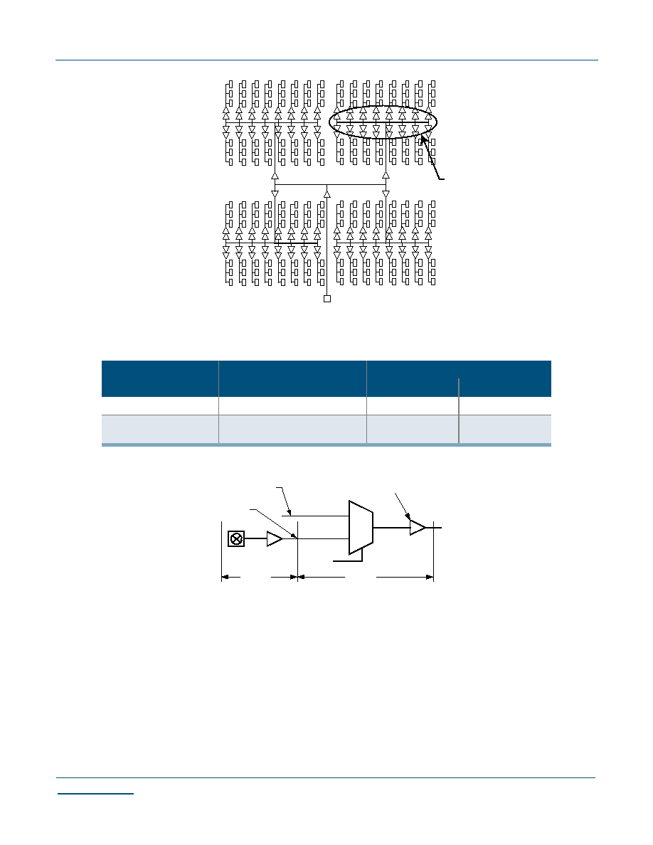
Figure 3: Logic Cell Flip-Flop
Figure 4: Logic Cell Flip-Flop Timings--First Waveform
Figure 5: Logic Cell Flip-Flop Timings--Second Waveform
SET
D
CLK
RESET
Q
SET
RESET
Q
CLK
tCWHI (min)
tCWLO (min)
tRESET
tRW
tSET
tSW
CLK
D
Q
tSU
tHL
tCO
www.quicklogic.com
© 2003 QuickLogic Corporation
∑
∑
∑
∑
∑
∑
QL7120 EclipsePlus Data Sheet Rev C
4
Figure 6: EclipsePlus Global Clock Structure
Figure 7: Global Clock Structure Schematic
Table 2: Eclipse Global Clock Tree Delays
Clock Segment
Parameter
Value (ns)
Max. Rise
Max. Fall
t
PGCK
Global clock pin delay to quad net
0.990
1.386
t
BGCK
Global clock buffer delay
(quad net to flip flop)
0.534
1.865
Quad net
Programmable Clock
External Clock
Global Clock Buffer
Global Clock
t
PGCK
t
BGCK
Clock
Select
© 2003 QuickLogic Corporation
www.quicklogic.com
∑
∑
∑
∑
∑
∑
QL7120 EclipsePlus Data Sheet Rev C
5
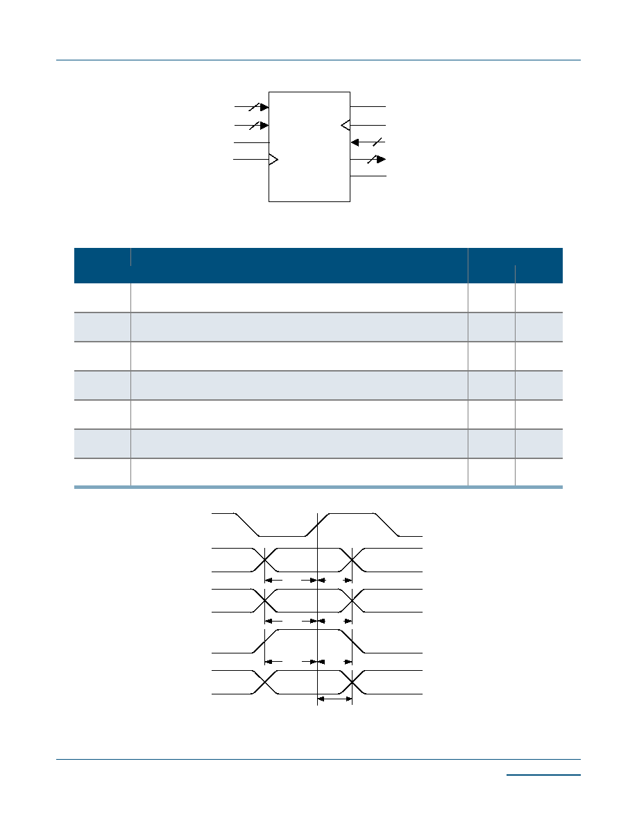
Figure 8: RAM Module
Figure 9: RAM Cell Synchronous Write Timing
Table 3: RAM Cell Synchronous Write Timing
Symbol
Parameter
Value (ns)
RAM Cell Synchronous Write Timing
Min
Max
t
SWA
WA setup time to WCLK: time the WRITE ADDRESS must be stable before the
active edge of the WRITE CLOCK
0.675 ns
-
t
HWA
WA hold time to WCLK: time the WRITE ADDRESS must be stable after the active
edge of the WRITE CLOCK
0 ns
-
t
SWD
WD setup time to WCLK: time the WRITE DATA must be stable before the active
edge of the WRITE CLOCK
0.654 ns
-
t
HWD
WD hold time to WCLK: time the WRITE DATA must be stable after the active edge
of the WRITE CLOCK
0 ns
-
t
SWE
WE setup time to WCLK: time the WRITE ENABLE must be stable before the active
edge of the WRITE CLOCK
0.276 ns
-
t
HWE
WE hold time to WCLK: time the WRITE ENABLE must be stable after the active
edge of the WRITE CLOCK
0 ns
-
t
WCRD
WCLK to RD (WA = RA): time between the active WRITE CLOCK edge and the
time when the data is available at RD
-
2.796 ns
WA
WD
WE
WCLK
RE
RCLK
RA
RD
RAM Module
[9:0]
[17:0]
[9:0]
[17:0]
ASYNCRD
tSWA
tSWD
tSWE
tHWA
tHWD
tHWE
tWCRD
old data
new data
WCLK
WA
WD
WE
RD