
© 2002 QuickLogic Corporation
∑
∑
∑
∑
∑
∑
∑ ∑ ∑ ∑ ∑ ∑
Preliminary
1
www.quicklogic.com
Device Highlights
LVDS SERDES Basic Features
∑
10 High Speed Bus LVDS Serial Links--
bandwidth up to 5 Gbps
∑
Eight Independent Bus LVDS serial
transceivers with operating speeds to 632
Mbps per channel
∑
Two Independent Bus LVDS clock serial
transceivers with operating speeds to
400 MHz per channel
∑
Integrated clock and data recovery (CDR)
with no external analog components
required
∑
CDR bypass for applications with external
clock source
∑
Programmable serial to parallel
configuration
∑
10-bit data width--with
∑
clock recovery
∑
4-bit, 7-bit and 8-bit data widths--
with external clock
∑
1-bit asynchronous level conversion
∑
Fast Lock and Random (auto) Lock capable
∑
Lock signal feedback
∑
I/O support for LVTTL, LVCMOS, PCI,
GTL+, SSTL2, SSTL3, LVDS, LVPECL
∑
Low Power/Independent power-down
mode for each SERDES channel
∑
IEEE1149.1 JTAG Support &
boundary scan
∑
Operation over PCB or backplane traces, or
across twisted pair cabling up to 25 m
∑
Point-to-Point, Multi-Point, and Multi-Drop
Support
∑
Pre-Emphasis Control on each LVDS
Channel Link
Extended Features
The following can be implemented into the
programmable logic:
∑
UTOPIA Level 2, 16-bit wide System
interface (up to 50 MHz) with parity support
for ATM applications
∑
UTOPIA Level 3 compatible 8-bit wide
system Interface (up to 100 MHz) with parity
support for ATM applications
∑
CSIX-L1 32-bit switch fabric interface (up to
100 MHz)
∑
Supports Generic 8,16,32-bit
microprocessor bus interface for
configuration, control and status monitoring
∑
Supports Generic 32, 64-bit peripheral bus
interface for bridging functions
Flexible Programmable Logic
∑
2,016 Programmable Logic Cells
∑
536 K System Gates
∑
Muxed architecture; non-volatile technology
∑
Completely customizable for any digital
application
Dual Port SRAM Blocks
∑
36 Dual Port SRAM Blocks
∑
Configurable array sizes (by 2, 4, 9, 18)
∑
< 3 ns access times, FIFO capable of over
300 MHz
∑
Configurable as RAM or FIFO
QL82SD Device Data Sheet
www.quicklogic.com
© 2002 QuickLogic Corporation
∑
∑
∑
∑
∑
∑
QL82SD Device Data Sheet Rev C
Preliminary
2
Programmable I/O
∑
Up to 252 Programmable I/O pins
∑
High performance Enhanced I/O (EIO): Less than 3 ns Tco
∑
Programmable Slew Rate Control
∑
Programmable I/O Standards
∑
LVTTL, LVCMOS, PCI, GTL+, SSTL2, and SSTL3, LVDS, LVPECL
∑
Four Independent I/O Banks
∑
Three Register Configuration: Input, Output, OE
Embedded Computational Unit (ECU) Blocks
∑
Integrated multiply, add, and accumulate function
∑
18 distributed MAC blocks
∑
8
◊
8 multiply (sign & unsigned)
∑
16-bit carry add
Advanced Clock Network
∑
Nine Global Clock Networks consisting of:
∑
one dedicated
∑
eight programmable
∑
Eight I/O (high drive) networks: two I/Os per bank
∑
Ten Quad-Net Networks--five per quadrant
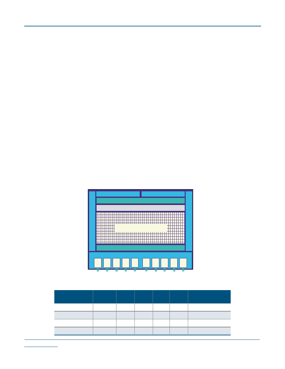
Figure 1: QL82SD Device Block Diagram
Table 1: QL82SD Device Table
Customer Part #
SERDES
Data
LVDS
Clocks
SRAM
Blocks
Logic
Cells
ECU
Blocks
Programmable I/O
QL82SD-PQ208
4
2
36
2016
18
75
QL82SD-PT280
8
2
36
2016
18
121
QL82SD-PS484
8
2
36
2016
18
209
QL82SD-PB516
8
2
36
2016
18
252
RAM Blocks
Embedded Computational Units (ECUs)
RAM Blocks
IO Block
IO Block
IO Block
2016 Logic Cells
CLKB
CH7
CH6
CH5
CH4
CH3
CH2
CH1
CH0
CLKA
LVDS/SERDES IO Block
IO Block
© 2002 QuickLogic Corporation
∑
∑
∑
∑
∑
∑
QL82SD Device Data Sheet Rev C
Preliminary
3
www.quicklogic.com
General Description
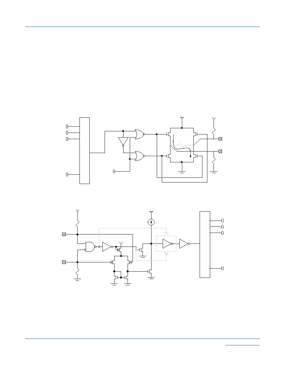
LVDS SERDES Transmitter and Receiver
A QuickSD LVDS SERDES device in serializer mode takes a parallel data bus and a separate
clock and converts them into a serial data stream. In deserializer mode, it takes a serial data
stream and converts it to a configurable bit wide parallel data bus and separate clock. The
reduced number of I/O board traces and cable connectors saves on cost and significantly
simplifies design. Skew and timing issues are significantly reduced and performance is
enhanced.
Figure 2
and
Figure 3
illustrate the block diagrams of the QuickSD device
transmitter and receiver.
Figure 2: LVDS SERDES Transmitter Block Diagram
Figure 3: LVDS SERDES Receiver Block Diagram
RL = 27 - 100
Vo +
Vo -
IL = 8-12 mA
Do +
Do -
300k
300k
/Enable
Parallel to Serial
.
.
.
.
txd [9:0]
TTL_Din
Din +
Din -
300k
W
300k
W
VCM = 0.2 V - 2.2 V
Serial to Parallel
.
.
.
.
FPGA
rxd [9:0]

www.quicklogic.com
© 2002 QuickLogic Corporation
∑
∑
∑
∑
∑
∑
QL82SD Device Data Sheet Rev C
Preliminary
4
LVDS SERDES Applications
The QuickSD device is designed to address the need for high-speed serial communications.
It maintains the features of standard discrete SERDES devices, but integrates these features
with customizable logic to allow for the highest degree of flexibility, performance, and
integration at the lowest cost. The QuickSD device is designed to support both transmit and
receive requirements in a single chip. The device can support multiple channels in a variety
of modes (with or without clock recovery,) a variety of translation widths (1:1 to 1:10), as
well as a range of frequencies. These capabilities make this device ideal in applications where
the performance is critical and customization is required.
The QuickSD device targets three applications: on-board, board-to-board (via common
backplane), and box-to-box (via common cable).
Software Support
The turnkey QuickWorks
package from QuickLogic
provides the most complete ESP and
FPGA software solution from design entry to logic synthesis, to place and route, and to
simulation. The package provides a solution for designers who use third-party tools from
Cadence, Mentor, OrCAD, Synopsys, Viewlogic, Veribest and other third-party tools for
design entry, synthesis, or simulation. A power calculator is also provided for SERDES power
consumption.
To speed up the QuickSD design process, QuickLogic includes a SERDES Wizard in its
QuickWorks package. This wizard simplifies the process of configuring the multi-channel
SERDES core into each of its modes. For details on the SERDES Wizard, please refer to "The
QL82SD Quickstart Design Guide". To find this guide go to the QuickSD device
documentation Web page at
h t t p : / / w w w. q u i ck l o g i c . c o m / h o m e . a s p ? Pag e I D = 3 1 5 &s M e n u I D= 1 9 9 # O rd e r
.
Process Data
QuickSD is fabricated on a 0.25
µ,
five-layer metal CMOS process. The core voltage is
2.5 Volt V
CC
supply and 3.3 V tolerant I/O with the addition of 3.3 Volt V
CCIO
. QuickSD is
available in commercial and industrial temperature grades.
© 2002 QuickLogic Corporation
∑
∑
∑
∑
∑
∑
QL82SD Device Data Sheet Rev C
Preliminary
5
www.quicklogic.com
Ordering Information
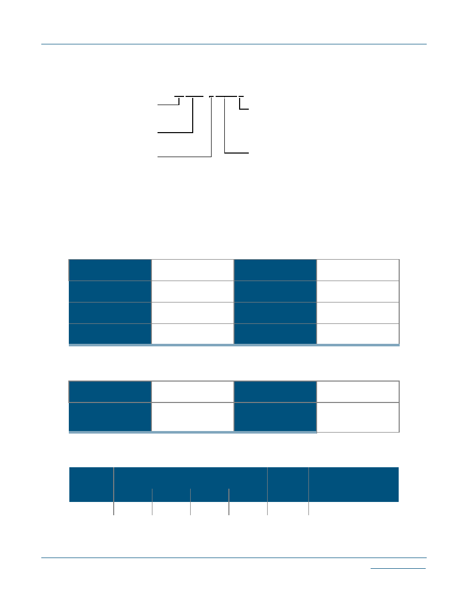
Maximum Ratings and Operating Range
Table 2: Absolute Maximum Electrical Ratings
V
CC
Voltage
-0.3 V to 4 V
Bus LVDS Driver
Output Voltage
-0.3 V to +2.8 V
LVCMOS/LVTTL
Input Voltage
-0.3 V to (V
CC
+ 0.3 V)
Bus LVDS Output Short
Circuit Duration
10 mS
LVCMOS/LVTTL
Output Voltage
-0.3 V to (V
CC
+ 0.3 V)
ESD Rating
HBM 2 kV
Bus LVDS Receiver
Input Voltage
-0.3 V to +2.8 V
Table 3: Absolute Maximum Thermal Ratings
Junction Temperature
+150∞C
Lead Temperature
(Soldering, 4 seconds)
+260∞C
Storage Temperature
-65∞C to +150∞C
Thermal and Power
Dissipation
Characteristics
See the following table
Table 4: Thermal and Power Dissipation Characteristics
Package
0
ja
(*C/W vs. Airflow
0
jc
(*C/W)
Estimated Maximum
Power Dissipation (W)
0.0
0.5
1.0
2.0
PQ208
26.0
24.5
23.0
22.0
11.0
1.65
QL 82SD - 4 PB516 C
QuickLogic device
QuickSD device
part number
Speed Grade
4 = Quick
5 = Fast
6 = Faster
7 = Fastest
Package Code
PQ208 = 208-pin FPBGA
PT280 = 280-pin BGA (1.0mm)
PS484 = 484-pin BGA (1.0mm)
PB516 = 516-pin BGA (1.27mm)
Operating Range
C = Commercial
I = Industrial
M = Military