 | –≠–ª–µ–∫—Ç—Ä–æ–Ω–Ω—ã–π –∫–æ–º–ø–æ–Ω–µ–Ω—Ç: QL8X12B-0 | –°–∫–∞—á–∞—Ç—å:  PDF PDF  ZIP ZIP |

QL8X12B
pASIC
Æ
1 Family
Very-High-Speed CMOS FPGA
4-5
Very High Speed ≠ ViaLink
Æ
metal-to-metal programmable≠via
antifuse technology, allows counter speeds over 150 MHz and logic
cell delays of under 2 ns.
High Usable Density ≠ An 8-by-12 array of 96 logic cells provides
1,000 usable ASIC gates (2,000 PLD gates) in 44-pin and 68-pin
PLCC, and 100-pin TQFP packages.
Low-Power, High-Output Drive ≠ Standby current typically 2 mA.
A 16-bit counter operating at 100 MHz consumes less than 50 mA.
Minimum IOL of 12 mA and IOH of 8 mA
Low-Cost, Easy-to-Use Design Tools ≠ Designs entered and
simulated using QuickLogic's new QuickWorks
Æ
development
environment, or with third-party CAE tools including Viewlogic,
Synopsys, Mentor, Cadence and Veribest. Fast, fully automatic place
and route on PC and workstation platforms using QuickLogic
software.
= Up to 56 prog. I/O cells, 6 Input high-drive cells, 2 Input/Clk (high-drive) cells
pASI
C 1
4
pASIC
HIGHLIGHTS
QL8x12B
Block Diagram
Rev B
...1,000
usable ASIC gates,
64 I/O pins
96 Logic Cells
QL8X12B
4-6
The QL8x12B is a member of the pASIC 1 Family of very-high-speed
CMOS user-programmable ASIC devices. The 96 logic cell field-
programmable gate array (FPGA) offers 1,000 usable "gate array" gates
(equivalent to 2,000 usable PLD gates) of high-performance general-
purpose logic in 44-pin and 68-pin PLCC packages and 100-pin TQFP
packages.
Low-impedance, metal-to-metal, ViaLink interconnect technology
provides nonvolatile custom logic capable of operating above 150 MHz.
Logic cell delays under 2 ns, combined with input delays of under 1.5 ns
and output delays under 3 ns, permit high-density programmable devices
to be used with today's fastest microprocessors and DSPs.
Designs can be entered using QuickLogic's QuickWorks Toolkit or most
populart third-party CAE tools. QuickWorks combines Verilog/VHDL
design entry and simulation tools with device-specific place & route and
programming software. Ample on-chip routing channels allow fast, fully
automatic place and route of designs using up to 100% of the logic and
I/O cells, while maintaining fixed pin-outs.
Total of 64 I/O pins
≠ 56 Bidirectional Input/Output pins
≠ 6 Dedicated Input/High-Drive pins
≠ 2 Clock/Dedicated input pins with fanout-independent, low-skew
clock networks
Input + logic cell + output delays under 6 ns
Chip-to-chip operating frequencies up to 110 MHz
Internal state machine frequencies up to 150 MHz
Clock skew < 0.5 ns
Input hysteresis provides high noise immunity
Built-in scan path permits 100% factory testing of logic and I/O cells
and functional testing with Automatic Test Vector Generation
(ATVG) software after programming
Available packages are 44- and 68-pin PLCC, and a 100-pin TQFP
68-pin PLCC compatible with QL12x16B
100-pin TQFP compatible with QL12x16B and QL16x24B
0.65µ CMOS process with ViaLink programming technology
PRODUCT
SUMMARY
FEATURES

QL8X12B
4-7
Pins identified I/SCLK, SM, SO and SI are used during scan path testing operation.
pASI
C 1
4
Pinout
Diagram
44-pin PLCC
Pinout
Diagram
68-pin PLCC

QL8X12B
4-8
Pinout Diagram
100-pin TQFP
QL8X12B
4-9
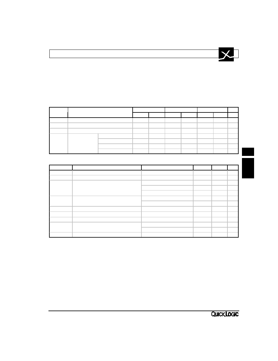
ABSOLUTE MAXIMUM RATINGS
Supply Voltage.................................. ≠0.5 to 7.0V
Storage Temperature....... ≠65∞C to + 150∞C
Input Voltage ....................... ≠0.5 to VCC +0.5V
Lead Temperature................................... 300∞C
ESD Pad Protection................................... ±2000V
DC Input Current ...................................... ±20 mA
Latch-up Immunity ................................ ±200 mA
OPERATING RANGE
DC CHARACTERISTICS over operating range
*IOL = 12 mA for commercial range only. IOL = 8 mA for the industrial and military ranges.
Notes:
[1]
Capacitance is sample tested only. CI = 20 pF max on I/(SI).
[2]
Only one output at a time. Duration should not exceed 30 seconds.
[3]
Commercial temperature grade only. Maximum Icc for industrial grade is 15mA and for military grade is
20 mA. For AC conditions use the formula described in the Section 9 -- Power vs Operating Frequency.
[4]
Stated timing for worst case Propagation Delay over process variation at VCC = 5.0V and TA = 25∞C.
Multiply by the appropriate Delay Factor, K, for speed grade, voltage and temperature settings as specified
in the Operating Range.
[5]
These limits are derived from a representative selection of the slowest paths through the pASIC logic cell
including net delays. Worst case delay values for specific paths should be determined from timing analysis
of your particular design .
pASI
C 1
4
Symbol
Parameter
Military
Industrial
Commercial
Unit
Min
Max
Min
Max
Min
Max
VCC
Supply Voltage
4.5
5.5
4.5
5.5
4.75
5.25
V
TA
Ambient Temperature
-55
-40
85
0
70
∞
C
TC
Case Temperature
125
∞
C
-X Speed Grade
0.4
2.75
0.46
2.55
K
Delay Factor
-0 Speed Grade
0.39
1.82
0.4
1.67
0.46
1.55
-1 Speed Grade
0.39
1.56
0.4
1.43
0.46
1.33
-2 Speed Grade
0.4
1.35
0.46
1.25
Symbol
Parameter
Conditions
Min
Max
Unit
VIH
Input HIGH Voltage
2.0
V
VIL
Input LOW Voltage
0.8
V
IOH = -4 mA
3.7
V
VOH
Output HIGH Voltage
IOH = -8 mA
2.4
V
IOH = -10
µ
A
VCC-0.1
V
VOL
Output LOW Voltage
IOL = 12 mA*
0.4
V
IOL = 10
µ
A
0.1
V
II
Input Leakage Current
VI = VCC or GND
-10
10
µ
A
IOZ
3-State Output Leakage Current
VI = VCC or GND
-10
10
µ
A
CI
Input Capacitance [1]
10
pF
IOS
Output Short Circuit Current [2]
VO = GND
-10
-80
mA
VO = VCC
30
140
mA
ICC
D.C. Supply Current [3]
VI, VIO = VCC or GND
10
mA