 | –≠–ª–µ–∫—Ç—Ä–æ–Ω–Ω—ã–π –∫–æ–º–ø–æ–Ω–µ–Ω—Ç: V370PDC | –°–∫–∞—á–∞—Ç—å:  PDF PDF  ZIP ZIP |

Copyright © 1999, V3 Semiconductor Corp.
V370PDC_A0 Data Sheet Rev 1.01 DS-PD01-0101
1
V370PDC
Rev. A0
High Performance PCI SDRAM Controller with
Integrated Peripheral Control Unit
V3 Semiconductor reserves the right to change the specifications of this product without notice.
V370PDC is a trademark of V3 Semiconductor Inc. All other trademarks are the property of their respective owners.
V 3 7 0 P D C
S D R A M
a n d P R O M
ISA
Conversion
Logic
P C I - t o - I S A C o n v e r s i o n
A p p l i c a t i o n
V 3 7 0 P D C
S D R A M
S R A M /
F L A S H
PCI Target Only
Application
∑ Fully compliant with PCI 2.2 specification target
interface
∑ Multiplexed or Non-multiplexed 8-, 16-, or 32-bit
generic peripheral bus interface
∑ Support up to 1 Gbyte of SDRAM
∑ Support up to 2 single banks or 1 dual bank
industrial standard 168-pin PC SDRAM DIMM
∑ Support up to 1Kbyte of burst access from PCI
∑ Up to 5 programmable chip select for peripheral
strobe generation
∑ Large On-Chip FIFOs using V3's unique
DYNAMIC BANDWIDTH ALLOCATIONTM
architecture
∑ Buffered PCI clock output
∑ Hot Swap Ready (PICMGTM Hot Swap
Specification)
∑ Implementation of PCI Bus Power Management
Interface Specification Version 1.0
∑ Initialization through PCI or serial EEPROM
∑ Programmable PCI and local interrupt
management
∑ Two 32-bit General Purpose Timers
∑ Up to 66 MHz local bus clock with asynchronous
PCI clock up to 33MHz
∑ 3.3V operation with 5V tolerant inputs
∑ Industrial Temperature Range (-40C to +85C)
∑ Low cost 160-pin PQFP package
The V370PDC PCI SDRAM Controller simplifies the
design of PCI based memory sub-systems. System
designers can replace many lower integration support
components with this single, high-integration device
saving design time, board area, and manufacturing
cost.
The V370PDC from V3 Semiconductor is a high
performance PCI SDRAM Controller with integrated
peripheral control unit operating at up to 66 MHz local
bus speed. It features multiple address translation
units from PCI which allow designers the freedom to
customize their local address space. Access latency of
slower peripherals are absorbed through the large On-
Chip FIFOs.
The peripheral bus provides low latency access to
SDRAM. The peripheral control unit on the V370PDC
also performs address decoding and chip-select
strobes generation for SRAM, PROM and other slow
peripherals. The peripheral bus can also be tri-stated
through a simple hand-shaking protocol to allow other
local bus masters control of the bus.
The SDRAM Controller connects the PCI bus through
on-chip FIFOs to SDRAM arrays of up to 1 Gbytes in
size. The fully programmable SDRAM controller also
supports the use of Enhanced SDRAM to achieve
even greater performance. Burst accesses of up to 1
Kbyte from PCI is supported.
The two g enera l pur pose 32-bit time rs ca n be
individually configured as a pulse width modulator, or
used in other modes such as retriggerable or one-
shot. Interrupts for a real time OS can be easily
generated by the system heartbeat timer. A watchdog
timer is also provided for graceful recovery from
catastrophic program failures. Interrupt requests for all
on-chip peripherals are managed by the Interrupt
Control Unit. Additionally, off-chip interrupts can be
routed to the Interrupt Control Unit.
The V370PDC is packaged in a low-cost 160-pin EIJA
Plastic Quad Flat Pack (PQFP), and is available in
66MHz speed grade.
TYPICAL APPLICATION
V370PDC
2
V370PDC_A0 Data Sheet Rev 1.01 DS-PD01-0101
Copyright © 1999, V3 Semiconductor Inc.
This document contains the product codes, pinout, package mechanical information, DC
characteristics, and AC characteristics for the V370PDC. Detailed functional information is contained
in the User's Manual.
V3 Semiconductor retains the rights to change documentation, specifications, or device
functionality at any time without notice. Please verify that you have the latest copy of all
documents before finalizing a design.
1.0 Product Codes
2.0 Pin Description
Table 2 below lists the pin types found on the V370PDC. Table 3 describes the function of each pin on
the V370PDC.
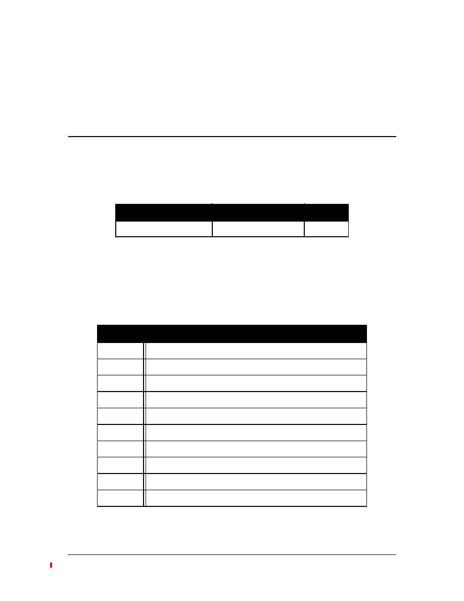
Table 1: Product Codes
Product Code
Package
Frequency
V370PDC-66 REV A0
160-pin EIAJ PQFP
66MHz
Table 2: Pin Types
Pin Type
Description
PCI I
PCI input only pin.
PCI O
PCI output only pin.
PCI I/O
PCI tri-state I/O pin.
PCI I/OD
PCI input with open drain output.
I/O
8
TTL I/O pin with 8mA output drive.
I/OD
TTL input with open drain output.
I
TTL input only pin.
O
2
TTL output pin with 2mA output drive.
O
8
TTL output pin with 8mA output drive.
O
12
TTL output pin with 12mA output drive.

V370PDC
Copyright © 1999, V3 Semiconductor Corp.
V370PDC_A0 Data Sheet Rev 1.01 DS-PD01-0101
3
Table 3: Signal Descriptions
PCI Bus Interface
Signal
Type
R
a
Description
AD[31:0]
PCI I/O
Z
Address and data, multiplexed on the same pins.
C/BE[3:0]
PCI I
Bus Command and Byte Enables, multiplexed on the same pins.
PAR
PCI I/O
Z
Parity represents even parity across AD[31:0] and C/BE[3:0].
FRAME
PCI I
Cycle Frame indicates the beginning and burst length of an
access.
IRDY
PCI I
Initiator Ready indicates the initiating agent's (bus master's) ability
to complete the current data phase of the transaction.
TRDY
PCI O
Z
Target Ready indicates the target agent's (selected device's) abil-
ity to complete the current data phase of the transaction.
STOP
PCI O
Z
Stop indicates the current target is requesting the master to stop
the current transaction (retry or disconnect).
DEVSEL
PCI O
Z
Device Select, when actively driven by a target, indicates the driv-
ing device has decoded its address as the target of the current
access.
IDSEL
PCI I
Initialization Device Select is used as a chip select during configu-
ration read and write transactions. It must be driven high in order
to access the chip's internal configuration space.
PERR
PCI I/O
Z
Parity Error is used to report data parity errors during all PCI
transactions except a Special Cycle.
SERR
PCI I/OD
Z
System Error is used to report address parity errors, data parity
errors on the Special Cycle command, or any other system error
where the result will be catastrophic.
PCLK
PCI I
PCLK provides timing for all transactions on the PCI bus.
SDRAM and Peripheral Bus Interface
Signal
Type
R
Description
CLKIN
I
Local clock input
CLKOUT
O
12
X
Buffered PCI clock output
DCS[3:0]
O
8
Z
SDRAM Chip Select
MA[14:0]
O
12
Z
SDRAM Memory Address (also, A[16:2] for peripheral access).
MA[14:13] are typically used for BA[1:0]
RAS
O
12
Z
SDRAM Row Address Strobe

V370PDC
4
V370PDC_A0 Data Sheet Rev 1.01 DS-PD01-0101
Copyright © 1999, V3 Semiconductor Inc.
CAS
O
12
Z
SDRAM Column Address Strobe
MWE
O
12
Z
SDRAM Memory Write Enable
MAD[31:0]
I/O
8
Z
SDRAM and peripheral bus data
DQM[3:0]
O
8
Z
SDRAM Data Mask (these act as MBE[3:0], A[1:0] for peripheral
access)
MARB_IN
I
Peripheral bus arbitration input: Treated as bus request input
when V370PDC is the primary bus master. When V370PDC is the
secondary bus master, this input acts as bus grant.
MARB_OUT
O
8
0
Peripheral bus arbitration output: Treated as bus grant output
when V370PDC is the primary bus master. When V370PDC is the
secondary bus master, this output acts bus request.
ALE
O
8
Z
Address Latch Enable: used to latch the address on MAD[31:0]
during the address phase of a peripheral bus access.
ADS
O
8
Z
Asserted low to indicate the beginning of a bus cycle.
BLAST
O
8
Z
Burst last.
READY
I
Data ready.
WNR
O
8
Z
Write/Read.
SDA
I/OD
Z
Serial EEPROM Data
SCL
O
2
Z
Serial EEPROM Clock
IOC[11:0]
I/O
8
Z
Multi-purpose I/O that can be configured for many functions
INT[3:0]
I/O
8
Z
General purpose interrupt inputs/outputs: may be used for either
PCI or local processor interrupts
Mode and Reset
Signal
Type
R
Description
RSTIN
I
Reset Input: Active low reset input used to initialize all internal
functions of the chip.
RSTOUT
O
8
0
Reset Output: Driven active when the input reset is driven active.
Driven inactive when the RSTOUT bit in the system register is set.
The RSTOUT signal is synchronous to the rising edge of CLKIN.
CH
I
PCI Precharge Bias: This signal is driven low to activate the on-
chip precharge bias for use in PICMG Hot Swap applications.
Non-Hot Swap applications should pull this signal high.
Table 3: Signal Descriptions (cont'd)

V370PDC
Copyright © 1999, V3 Semiconductor Corp.
V370PDC_A0 Data Sheet Rev 1.01 DS-PD01-0101
5
2.1
Pinout
Table 4 lists the pins by pin number. Figure 1 shows the pinout for the 160-pin EIAJ PQFP package
and Figure 2 shows the mechanical dimensions of the package
MODE
I
MODE Input: selects mastership of V370PDC
:
0 = Secondary master
1 = Primary master
Power and Ground Signals
Signal
Type
R
Description
V
CC
-
POWER leads for external connection to a 3.3V V
CC
board plane.
GND
-
GROUND leads for external connection to a GND board plane.
NC
-
No connect.
a. R indicates state during reset.
Table 3: Signal Descriptions (cont'd)