 | –≠–ª–µ–∫—Ç—Ä–æ–Ω–Ω—ã–π –∫–æ–º–ø–æ–Ω–µ–Ω—Ç: V3xxEPC | –°–∫–∞—á–∞—Ç—å:  PDF PDF  ZIP ZIP |

© 2000 V3 Semiconductor Corp.
V363EPC A0 Data Sheet Rev 1.01
DS-EC301-0101
1
V363EPC A0 Local Bus to PCI Bridge
for Embedded Processors
1.0
About the V363EPC
V363EPC A0 Data Sheet
w
Direct interface to these processors:
∑ AMD
Æ
AM29030/40TM
∑ IBM
Æ
PowerPC 401TM Gx
∑ Intel
Æ
i960
Æ
Cx/Hx/Jx/Sx
w
Fully compliant with PCI Local Bus
Specification, Revision 2.1
w
Configurable for system master, PCI bus
master, or PCI target operation
w
Type 0 and Type 1 PCI configuration cycles
w
Up to 1 kB burst access on the PCI or
the local bus
w
640 bytes of programmable FIFO storage with
Dynamic Bandwidth AllocationTM architecture
w
64-byte read FIFO in each direction
w
Enhanced support for 8-bit/16-bit local bus
devices with programmable region sizes
w
Dual bi-directional address space remapping
w
10-bit bus watch timer
w
On-the-fly byte order (endian) conversion
w
I
2
O-ReadyTM ATU and messaging unit,
including hardware controlled circular queues
w
Two-channel DMA, multiprocessor DMA
chaining, and demand mode DMA
w
Hot Swap CapableTM according to the PICMG
Æ
Hot Swap Specification, version 2.1
w
Sixteen 8-bit bi-directional mailbox registers
with doorbell interrupts
w
Support for real-mode MS-DOS
Æ
holes
w
Flexible PCI and local interrupt management
w
Optional power-on serial EEPROM
initialization
w
Up to 50 MHz on both PCI and local bus clocks
w
3.3 V operation; 5 V tolerant input
w
Industrial temperature range (
-
40∞C to +85∞C)
w
Low-cost 160-pin EIAJ PQFP package
(Electronic Industries Association of Japan
Plastic Quad Flat Pack)

About the V363EPC
2
V363EPC A0 Data Sheet Rev 1.01
DS-EC301-0101
© 2000 V3 Semiconductor Corp.
The V363EPC offers the highest performance, most flexible, and most economical solution for interfacing either
32-bit or 16-bit local bus applications to the PCI bus. It is also an ideal candidate for a variety of high-performance
applications based on Motorola, IBM, DEC, Hitachi, and other popular embedded processors where only a minimal
amount of glue logic is needed.
V363EPC is the 3.3 V enhanced version of the V350EPC and V360EPC Rev A1 devices and supports powerful
features like Hot Swap and DMA chaining. The PCI bus operates at up to 50 MHz, independent of local bus clock
frequency. The overall throughput of the system is dramatically improved by using our unique Dynamic Bandwidth
AllocationTM architecture.
Access to the PCI bus can be performed through two programmable address apertures. Two more apertures are
provided for PCI-to-local bus accesses. There are 64 bytes of read FIFOs in each direction, 32 bytes dedicated for
each aperture.
Two high-performance DMA channels with chaining and demand mode capabilities provide a powerful data transfer
engine for bulk data transfers. Mailbox registers and flexible PCI interrupt controllers also provide a simple
mechanism to emulate PCI device control ports. The part is available in a 160-pin, low-cost PQFP package.
This document contains the product codes, pinouts, package mechanical information, DC characteristics, and AC
characteristics for the V363EPC. Detailed functional information is contained in the User's Manual.
Note:
V3 Semiconductor retains the rights to change documentation, specifications, or
device functionality at any time without notice. Please verify that you have the latest copy
of all documents before finalizing a design.

Product Codes
© 2000 V3 Semiconductor Corp.
V363EPC A0 Data Sheet Rev 1.01
DS-EC301-0101
3
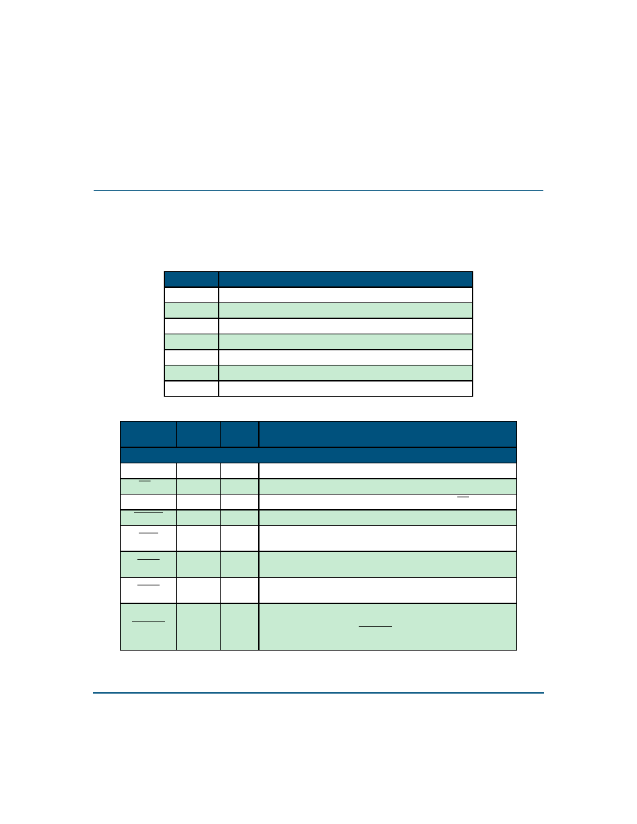
Figure 1: Example Applications
2.0
Product Codes
Table 1: Product Codes
Product Code
Package
Frequency
V363EPC-50 REV A0 160-pin EIAJ PQFP
50 MHz
CPU
PCI Edge Connector
SCSI
Controller
Card acts as a bus
master; it receives
and transmits data
on the PCI bus
Hard
Disk
Graphics
Engine
PCI Edge Connector
Frame Buffer
and RAMDAC
Card is never a bus
master and receives
video data from
other masters
To
Monitor
V363EPC
CPU
PCI Bus
PCI Target
Add-In
Card
PCI Target
Add-In
Card
PCI Target
Add-In
Card
V363EPC
V380SDC
SDRAM
Controller
PCI Bus
SDRAM
V363EPC
I
2
O Ready
V363EPC
I
2
O Ready
Pin Descriptions and Pinouts
4
V363EPC A0 Data Sheet Rev 1.01
DS-EC301-0101
© 2000 V3 Semiconductor Corp.
3.0
Pin Descriptions and Pinouts
Table 2
lists the pin types found on the V363EPC. Together,
Table 3
and
Table 4
describe the function of each pin on
the V363EPC.
Table 5
lists the RESET state for test mode pins.
Section 3.2
lists processor-mode-specific pin
assignments and shows the pinouts for the 160-pin EIAJ PQFP package.
Figure 6
shows the mechanical dimensions
of the package.
Table 2: Pin Types
Pin Type
Description
PCI I
PCI input only pin.
PCI O
PCI output only pin.
PCI I/O
PCI tri-state I/O pin.
PCI I/O
D
PCI input with open drain output.
I/O
4
TTL I/O pin with 4 mA output drive.
I
TTL input only pin.
O
4
TTL output pin with 4 mA output drive.
Table 3: Signal Descriptions: Non-Processor Mode Dependent
Signal
Type
Reset
State
Description
PCI Bus Interface Signals
AD[31:0]
PCI I/O
Z
Address and Data multiplexed on the same pins.
C/BE[3:0]
PCI I/O
Z
Bus Command and Byte Enables multiplexed on the same pins.
PAR
PCI I/O
Z
Parity represents even parity across AD[31:0] and C/BE[3:0].
FRAME
PCI I/O
Z
Cycle Frame indicates the beginning and burst length of an access.
IRDY
PCI I/O
Z
Initiator Ready indicates the initiating agent's (bus master's) ability
to complete the current data phase of the transaction.
TRDY
PCI I/O
Z
Target Ready indicates the target agent's (selected device's) ability
to complete the current data phase of the transaction.
STOP
PCI I/O
Z
Stop indicates that the current target is requesting the master to stop
the current transaction (retry or disconnect).
DEVSEL
PCI I/O
Z
Device Select, when actively driven by a target, indicates the driving
device has decoded its address as the target of the current access.
As an input to the initiator, DEVSEL indicates whether any device on
the bus has been selected.
Pin Descriptions and Pinouts
© 2000 V3 Semiconductor Corp.
V363EPC A0 Data Sheet Rev 1.01
DS-EC301-0101
5
IDSEL
PCI I
Initialization Device Select is used as a chip select during
configuration read and write transactions. It must be driven high in
order to access the chip's internal configuration space.
REQ
PCI O
Z
Request indicates to the arbiter that this agent requests use of the
bus.
GNT
PCI I
Grant indicates to the agent that access to the bus has been
granted.
PCLK
PCI I
PCI Clock provides timing for all transactions on the PCI bus.
PRST
PCI I/O
Z/L
PCI Reset acts as an input when RDIR is high, an output when
RDIR is low. As an input it is asserted low to bring all internal EPC
operation to a reset state.
PERR
PCI I/O
Z
Parity Error is used to report data parity errors during all PCI
transactions except a Special Cycle.
SERR
PCI I/OD
Z
System Error is used to report address parity errors, data parity
errors on the Special Cycle command, or any other system error
where the result will be catastrophic.
INT[A:D]
PCI I/OD
Z
Interrupt is used to receive or generate level-sensitive interrupt
requests.
Serial EEPROM Interface Signals
SCL/LPERR
O
4
X
EEPROM Clock, Local Parity Error.
SDA
I/O
4
X
EEPROM Data.
Configuration Signal
RDIR
I
Reset Direction: tie low to drive PRST out and LRST in; tie high to
drive LRST out and PRST in.
Power and Ground Signals
V
CC
--
Power leads for external connection to a 3.3 V V
CC
board plane.
GND
--
Ground leads for external connection to a GND board plane.
Table 3: Signal Descriptions: Non-Processor Mode Dependent
Signal
Type
Reset
State
Description