 | –≠–ª–µ–∫—Ç—Ä–æ–Ω–Ω—ã–π –∫–æ–º–ø–æ–Ω–µ–Ω—Ç: V962PBC | –°–∫–∞—á–∞—Ç—å:  PDF PDF  ZIP ZIP |
Copyright © 1998, V3 Semiconductor Inc.
V962PBC Data Sheet Rev 2.4
1
V962PBC
Rev. B2
LOCAL BUS TO PCI BRIDGE
FOR DE-MULTIPLEXED A/D PROCESSORS
V3 Semiconductor reserves the right to change the specifications of this product without notice.
V962PBC and V96BMC are trademarks of V3 Semiconductor. All other trademarks are the property of their respective owners.
∑ Glueless interface between Intel i960 Cx/Hx
processors and PCI bus
∑ Fully compliant with PCI 2.1 specification
∑ Configurable for primary master, bus master, or
target operation
∑ Up to 1Kbyte burst access support on both local
and PCI interface
∑ 576 bytes of programmable FIFO storage with
D
YNAMIC
B
ANDWIDTH
A
LLOCATION
TM
∑ Two channel DMA controller
∑ Enhanced support for 8/16-bit local bus devices
with programmable region size register
∑ 16 8-bit bi-directional mailbox registers with
doorbell interrupts
∑ Dual bi-directional address space remapping
∑ On-the-fly byte order (endian) conversion
∑ Optional power on serial EEPROM initialization
∑ I
2
O ATU and messaging unit including
hardware controlled circular queues
∑ Flexible PCI and local interrupt management
∑ Support for real-mode DOS "holes"
∑ Ability to generate both Type 0 and Type 1
configuration cycles
∑ 33MHz and 40MHz local bus versions available
with independent PCI operation up to 33MHz
∑ Low cost 160-pin EIAJ PQFP package
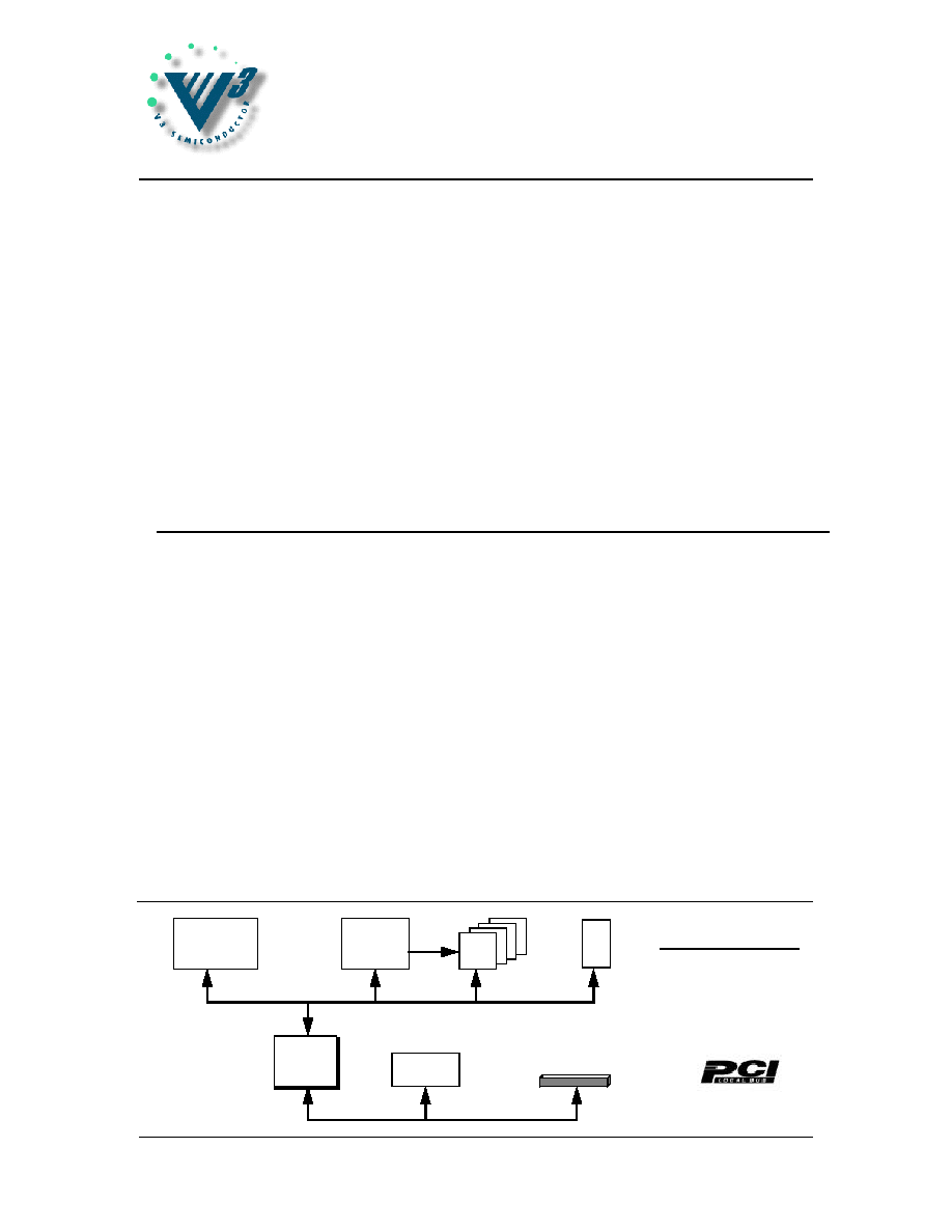
V962PBC provides the highest performance,
most flexible, and most economical method to
directly connect i960Cx/Hx processors to the PCI
bus. V292PBC is also a suitable candidate for
a variety of 32-bit de-multiplexed local bus
a p p l i c a t i o n s b a s e d o n i n t e l e m b e d d e d
processors - where a minimal amount of glue
logic is required. V962PBC may also be used in
systems without a CPU for a generic PCI master/
target interface.
V962PBC Rev B2 is the first I2O ready PCI
bridge, fully backward compatible with V962PBC
Rev B1. The PCI bus can be run at the full
33MHz frequency, independent of local bus
clock rate. The overall throughput of the system
is dramatically improved by increasing the FIFO
d e p t h a n d u t i l i z i n g t h e u n i q u e
D
Y N A M I C
B
ANDWIDTH
A
LLOCATION
TM architecture.
Access to the PCI bus can be performed through
two programmable address apertures. Two more
apertures are provided for PCI-to-local bus
accesses. There are 32-bytes of read FIFO's in
each direction, 16-byte dedicated for each
aperture. V962PBC also includes bi-directional
remapping capabilities, and on-the-fly byte order
conversion
Two DMA channels are provided for autonomous
PCI-to-Local/Local-to-PCI transfers. Mailbox
registers and flexible PCI interrupt controllers are
also included to provide a simple mechanism to
emulate PCI device control ports.
The part is available in 160-pin low cost EIAJ
Plastic Quad Flat Pack (PQFP) package.
i960Cx/Hx
CPU
V96BMC
MEMORY
CONTROL
D
R
A
M
ROM
V962PBC
LOCAL TO
PCI BRIDGE
TYPICAL APPLICATION
PERIPHERAL
PCI
PCI SLOT or EDGE CONNECTOR
V962PBC
2
V962PBC Data Sheet Rev 2.4
Copyright © 1998, V3 Semiconductor Inc.
This document contains the product codes, pinouts, package mechanical information, DC
characteristics, and AC characteristics for the V962PBC. Detailed functional information is contained
in the User's Manual.
V3 Semiconductor retains the rights to change documentation, specifications, or device
functionality at any time without notice. Please verify that you have the latest copy of all
documents before finalizing a design.
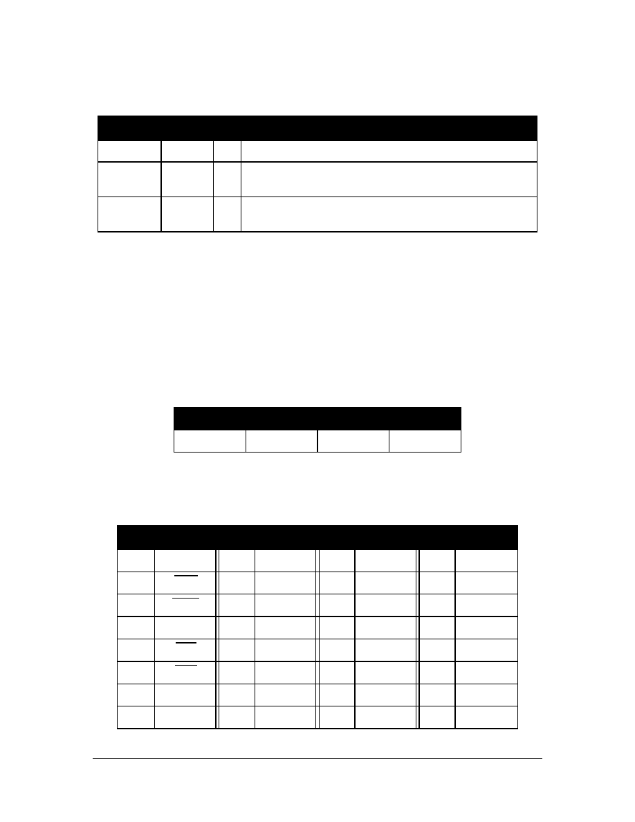
1.0 Product Codes
2.0 Pin Description and Pinout
Table 2 below lists the pin types found on the V962PBC. Table 3 describes the function of each pin on
the V962PBC. Table 5 lists the pins by pin number. Figure 1 shows the pinout for the 160-pin EIAJ
PQFP package and Figure 2 shows the mechanical dimensions of the package.
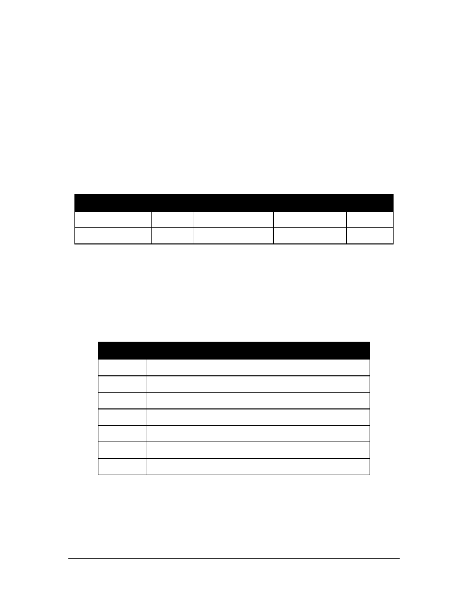
Table 1: Product Codes
Product Code
Processor
Bus Type
Package
Frequency
V962PBC-33 REV B2
i960Cx/Hx
32-bit de-multiplexed
160-pin EIAJ PQFP
33MHz
V962PBC-40 REV B2
i960Cx/Hx
32-bit de-multiplexed
160-pin EIAJ PQFP
40MHz
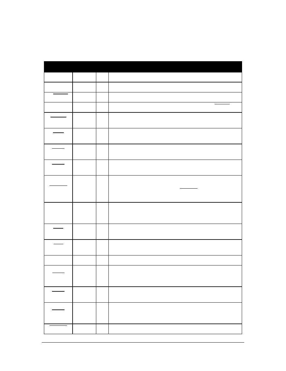
Table 2: Pin Types
Pin Type
Description
PCI I
PCI input only pin.
PCI O
PCI output only pin.
PCI I/O
PCI tri-state I/O pin.
PCI I/OD
PCI input with open drain output.
I/O
4
TTL I/O pin with 4mA output drive.
I
TTL input only pin.
O
4
TTL output pin with 4mA output drive.
V962PBC
Copyright © 1998, V3 Semiconductor Inc.
V962PBC Data Sheet Rev 2.4
3
Table 3: Signal Descriptions
PCI Bus Interface
Signal
Type
R
a
Description
AD[31:0]
PCI I/O
Z
Address and data, multiplexed on the same pins.
C/BE[3:0]
PCI I/O
Z
Bus Command and Byte Enables, multiplexed on the same pins.
PAR
PCI I/O
Z
Parity represents even parity across AD[31:0] and C/BE[3:0].
FRAME
PCI I/O
Z
Cycle Frame indicates the beginning and burst length of an
access.
IRDY
PCI I/O
Z
Initiator Ready indicates the initiating agent's (bus master's) ability
to complete the current data phase of the transaction.
TRDY
PCI I/O
Z
Target Ready indicates the target agent's (selected device's) abil-
ity to complete the current data phase of the transaction.
STOP
PCI I/O
Z
Stop indicates the current target is requesting the master to stop
the current transaction (retry or disconnect).
DEVSEL
PCI I/O
Z
Device Select, when actively driven by a target, indicates the driv-
ing device has decoded its address as the target of the current
access. As an input to the initiator, DEVSEL indicates whether
any device on the bus has been selected.
IDSEL
PCI I
Initialization Device Select is used as a chip select during configu-
ration read and write transactions. It must be driven high in order
to access the chip's internal configuration space.
REQ
PCI O
H
Request indicates to the arbiter that this agent requests use of the
bus.
GNT
PCI I
Grant indicates to the agent that access to the bus has been
granted.
PCLK
PCI I
PCLK provides timing for all transactions on the PCI bus.
PRST
PCI I/O
Z/L
Acts as an input when RDIR is high, an output when RDIR is low.
As an input it is asserted low to bring all internal PBC operation to
a reset state.
PERR
PCI I/O
Z
Parity Error is used to report data parity errors during all PCI
transactions except a Special Cycle.
SERR
PCI I/OD
Z
System Error is used to report address parity errors, data parity
errors on the Special Cycle command, or any other system error
where the result will be catastrophic.
INT[A:D]
PCI I/OD
Z
Level-sensitive interrupt requests may be received or generated.
V962PBC
4
V962PBC Data Sheet Rev 2.4
Copyright © 1998, V3 Semiconductor Inc.
Local Bus Interface
Signal
Type
R
Description
LD[31:0]
I/O4
Z
Local multiplexed address and data bus.
LA[31:2]
I/O4
Z
Local address bus.
BE[3:0]
I/O4
Z
Local bus byte enables.
W/R
I/O4
Z
Write/Read.
ADS
I/O4
Z
Asserted low to indicate the beginning of a bus cycle.
READY
I/O4
Z
Local Bus data ready
HOLD
O4
L
Local bus hold request: asserted by the chip to initiate a local bus
master cycle.
HOLDA
I
Local bus hold acknowledge.
LPAR[3:0]
I/O4
Z
Local bus parity.
BLAST
I/O4
Z
Burst request. Burst last.
BTERM
I/O4
Z
Bus Time-out. Burst terminate.
LINT
O4
H
Local interrupt request.
LRST
I/O4
L/Z
Local bus RESET signal.
LCLK
I
Local bus clock.
Serial EEPROM Interface
Signal
Type
R
Description
SCL/LPERR
O4
X
EEPROM clock. Local parity error.
SDA
I/O4
X
EEPROM data.
Configuration
Signal
Type
R
Description
RDIR
I
Reset direction. Tie low to drive PRST out and LRST in, high to
drive LRST out and PRST in.
Table 3: Signal Descriptions (cont'd)
V962PBC
Copyright © 1998, V3 Semiconductor Inc.
V962PBC Data Sheet Rev 2.4
5
2.1
Test Mode Pins
Several device pins are used during manufacturing test to put the V962PBC device into various test
modes.
These pins must be maintained at proper levels during reset to insure proper operation.
This is typically handled through pull-up or pull-down resistors (typically 1K to 10K) on the signal pins if
they are not guaranteed to be at the proper level during reset. Table 4 below shows the reset states for
test mode pins:
Power and Ground Signals
Signal
Type
R
Description
V
CC
-
POWER leads intended for external connection to a V
CC
board
plane.
GND
-
GROUND leads intended for external connection to a GND board
plane.
a.
R indicates state during reset.
Table 4: RESET State for Test Mode Pins
PIN#
134
135
153
Connection
Pull-Up
Pull-Up
Pull-Up
Table 5: Pin Assignments
PIN #
Signal
PIN #
Signal
PIN #
Signal
PIN #
Signal
1
V
CC
41
V
CC
81
V
CC
121
V
CC
2
INTD
42
AD14
82
LA23
122
LA6
3
PRST
43
AD13
83
LD8
123
LD25
4
PCLK
44
AD12
84
LA22
124
LA5
5
GNT
45
AD11
85
LD9
125
LD26
6
REQ
46
AD10
86
LA21
126
LA4
7
AD31
47
AD9
87
LD10
127
LD27
8
AD30
48
AD8
88
LA20
128
LA3
Table 3: Signal Descriptions (cont'd)