 | –≠–ª–µ–∫—Ç—Ä–æ–Ω–Ω—ã–π –∫–æ–º–ø–æ–Ω–µ–Ω—Ç: SY02-HLPL | –°–∫–∞—á–∞—Ç—å:  PDF PDF  ZIP ZIP |

SYNCHRONOUS EQUIPMENT
HIGH FREQUENCY HITLESS SYNCHRONIZER - SY02-HLPL
RALTRON ELECTRONICS CORP. 10651 N.W.19
th
St Florida 33172 U.S.A.
Tel: 305 593-6033 Fax: 305-594-3973 e-mail: sales@raltron.com Internet: http:/www.raltron.com
1
SY02-HLPL
PRELIMINARY SPECIFICATION
Date: July 1, 2002
∑
INTRODUCTION
The SY02-HLPL is a dual input reference hitless switching
device with high frequency crystal-based PLL synchronizer
designed as a subsystem module. Mainly used at high speed
Line Interface Cards in telecommunication products mainly
related to STN-n or OC-n. The SY02-HLPL is a
synchronization solution for timing and jitter topics specified
within ITU-T Recommendations G.813, ETSI -ETS 300 462-
4, and Bellcore GR-1244-CORE.
∑
FEATURES
-
Low jitter output from intrinsically low jitter VCXO or VCSO;
-
Two input references from
8KHz to 77.76MHz
(See page 3 for options)
-
One high frequency LVPECL output with enable/disable function up to
800MHz
(pre-select frequency value ≠
See page 3 for options)
-
Alarms and status;
-
Provides free running clock output;
-
Provides a manual input frequency selection
-
The unit changes timing modes in response to external events;
-
J-TAG service port for re-programming and servicing;
-
3.3V DC power supply
-
Small dimensions: 0.96" x 1.050"
∑
APPLICATIONS
-
ATM
-
SDH
-
PDH
-
SONET
-
Other telecommunication equipment.

SYNCHRONOUS EQUIPMENT
HIGH FREQUENCY HITLESS SYNCHRONIZER - SY02-HLPL
RALTRON ELECTRONICS CORP. 10651 N.W.19
th
St Florida 33172 U.S.A.
Tel: 305 593-6033 Fax: 305-594-3973 e-mail: sales@raltron.com Internet: http:/www.raltron.com
2
MUX,
FPD,
Counters
&
Logic
LOOP
FILTER
VCXO
FR
REF 1 IN
FRS
OUT
J-TAG PORT
OUT
EN OUT
ALARM
REF 2 IN
CNT
∑
DESCRIPTION
The SY02-HLPL synchronization module is a high frequency PLL that performs hitless switching plus additional
features necessary for timing at high-speed Line Interface Cards. The functional block diagram is shown in the
figure above . The SY02-HLPL receives two reference signals, from 8KHz to 77.76MHz (See page 3 for available
options) and using PLL synthesizer generates a high frequency signal necessary for transceivers or framers. The
PLL that is complemented by high-speed logic that provide processing, switching between the timing modes, alarm
and status messages and etc. A high quality VCXO provides very low jitter at the output.
The SY02-HLPL incorporates a High Frequency Phase Lock Loop has been designed to generate high frequency
(up to 800MHz) output from a low jitter VCXO (Crystal Based Oscillator) or VCSO (SAW based oscillators). The
output can be disabled externally by setting OUTEN pin high. The module supports a MANUAL operating mode
where unit will switch according to a control pin CNT. During an event where the external reference signal
disappears, the user instruct a reference change into the module through the control pin. The ALARM output signals
monitor the status of the phase loop LOL (Loss of Lock) and LOR (Loss of Reference). If the reference REF IN is
absent, the SY02-HLPL will automatically switch to free run mode and FRS output will indicate it. The SY02-HLPL is
provided in an SMD package dimensions are 0.96x1.050 inch and power supply is 3.3V.
- OUTPUT PROGRAMMING
OUTEN FR
OUTPUT
0
0
Locked to Reference
1 X
Output
Disabled
0 1 Free-Run
- ALARM STATES
LOL LOR
ALARM
0
0
No alarm
1 0
1
0 1
1
- Input Reference Selection
CNT
Input Reference Selection
0
Ext Ref 1
1
Ext Ref 2
SYNCHRONOUS EQUIPMENT
HIGH FREQUENCY HITLESS SYNCHRONIZER - SY02-HLPL
RALTRON ELECTRONICS CORP. 10651 N.W.19
th
St Florida 33172 U.S.A.
Tel: 305 593-6033 Fax: 305-594-3973 e-mail: sales@raltron.com Internet: http:/www.raltron.com
3
∑
PIN DESCRIPTION
Name Description
Signal
Technology
VL
VH/ DC Voltage
Min Typ Max
Min Typ
Max
1
ENABLE
Output Enable - > the input pin to enable the output,
active low
DC
0 0.25
(0.15)
0.5
(0.3)
4.5
(2.97)
5.0
(3.3)
5.25
(3.465)
2
TCK
J-TAG port for factory usage ≠ TCK
----- ----- ----- ----
------
------ ------
3
TDO
J-TAG port for factory usage ≠ TDO
----- ----- ----- ----
------
------ ------
4
REFA IN
Reference A Input -> Reference A input signal
HCMOS
(3.3 Tolerable)
0 ----- 0.5
(0.3)
4.5
(2.97)
---- ----
5
SEL
Select Input Reference -> input to select A (SEL=0) or B
(SEL=1)
DC
0 0.25
(0.15)
0.5
(0.3)
4.5
(2.97)
5.0
(3.3)
5.25
(3.465)
6
RESET
Reset input -> Reset active high
In normal operation must be Grounded
DC 0 0.25
(0.15)
0.5
(0.3)
4.5
(2.97)
5.0
(3.3)
5.25
(3.465)
7
REFB IN
Reference B Input -> Reference B input signal
HCMOS
(3.3 Tolerable)
0 ----- 0.5
(0.3)
4.5
(2.97)
---- ----
8 GND
Ground
----- ----- ----- ----
------
------ ------
9
FRS
Free-Run Status -> Output indicates that the module is in
free run, active high
DC 0 0.25
(0.15)
0.5
(0.3)
4.5
(2.97)
5.0
(3.3)
5.25
(3.465)
10
Vcc
Positive supply voltage
DC ≠ 5V
(3.3V)
4.5
(2.97)
5.0
(3.3)
5.25
(3.465)
11 NC
Not
Connected
----- ----- ----- ----
------
------ ------
12
ALARM
Alarm out -> Alarm output indicates loss of reference or
loss of lock ≠ High when the unit is Unlocked
DC 0 0.25
(0.15)
0.5
(0.3)
4.5
(2.97)
5.0
(3.3)
5.25
(3.465)
13
FR
Free-Run -> Control input to select free run of the
module, active high
DC 0 0.25
(0.15)
0.5
(0.3)
4.5
(2.97)
5.0
(3.3)
5.25
(3.465)
14
TDI
J-TAG port for factory usage ≠ TDI
----- ----- ----- ----
------
------ ------
15
TMS
J-TAG port for factory usage ≠ TMS
----- ----- ----- ----
------
------ ------
16
OUT
Oscillator Output -> Output of the module
LV/PECL
Vcc-1.680 Vcc-1.620 Vcc-1.560 Vcc-1.085
Vcc-1.025 Vcc-0.885
17 GND
Ground
----- ----- ----- ----
------
------ ------
18 OUT Complimentary
Output
LV/PECL
Vcc-1.680 Vcc-1.620 Vcc-1.560 Vcc-1.085
Vcc-1.025 Vcc-0.885
∑
ORDERING INFORMATION
o
Input Frequencies available;
Frequency Suffix Frequency Suffix Frequency Suffix
8KHz F8
19.44MHz
O1
77.76MHz
O3
1.544MHz T1 24.704MHz T3
2.048MHz E1 32.768MHz E4
8.192MHz E2 38.88MHz O2
12.352MHz T2 51.84MHz D1
16.384MHz E3 62.50MHz G1
o
Output Frequencies available (in MHz);
Frequency Suffix Frequency Suffix
51.84 D1 156.25 G4
62.50 G1
166.328
C1
77.76 O3 622.08 O5
125 G2
666.513
C2
133 G3
155.52 O4

SYNCHRONOUS EQUIPMENT
HIGH FREQUENCY HITLESS SYNCHRONIZER - SY02-HLPL
RALTRON ELECTRONICS CORP. 10651 N.W.19
th
St Florida 33172 U.S.A.
Tel: 305 593-6033 Fax: 305-594-3973 e-mail: sales@raltron.com Internet: http:/www.raltron.com
4
P/N System
SY02-FEC ≠ IP < Input Frequency> - OU<Output Frequency>-S-T<Temp. Range>-C <Cover Option>
See above Chart
If not listed Place
NL
and state
the Freq.)
See above Chart
(If Output Freq. Not applied place
NA
and state the Freq.)
Supply Voltage;
2
- 5V
4
≠ 3.3V
Operating Temperature Range;
C
-
0∞C to 70∞C
I
-40∞C to +85∞C
Cover Option;
M
≠ Metal Cover
N
- Non Covered unit
For other Options please contact the factory
∑
SPECIFICATION
General
Specifications
Mechanical
0.96" x 1.050"
SMT Module FR4 18 pins dual-in-line
Power
3.3VDC, <200mA
Regulated
Environment
Operating Temperature
0∞C to 70∞C
Humidity
5% to 95% non-condensing
Internal Oscillators
VCXO or VCSO
Depend of the frequency
Input Signals
Number of Reference Inputs
2
See page 3 for input frequencies
Input reference frequency
User select
See page 3 for input frequencies
Signal Level
LVCMOS
Voh; 2.97V min ; Vol; 0.33Vmax
Output Signals
Number of Outputs
1
Output 1
User select
See page 3 for output frequencies
Output 1 Signal Level
LVPECL (W/ Complimentary option)
Voh; 2.272V min ; Vol; 1.68Vmax
Duty Cycle
50+/-10%
50%+/-5% available upon request
Tracking/Capture
Range
±50ppm APR min
Free Run stability
±30ppm (VCXO)
±150PPM(VCSO)
T=+25C; Vcc/load-=nominal
Signal Quality
Performance
Jitter generation
<0.001UI RMS
<0.001UI RMS
<0.0001 UI RMS
<0.0001 UI RMS
HPF 30Hz
HPF 500Hz
HPF 12KHz
HPF 100KHz
Jitter
attenuation
-40dB
-10dB
Fj=10Hz~1KHz
Fj=1KHz~10MHz
Jitter
tolerance
2
µs, 10 Hz (0.05 UI @ 8KHz)
SYNCHRONOUS EQUIPMENT
HIGH FREQUENCY HITLESS SYNCHRONIZER - SY02-HLPL
RALTRON ELECTRONICS CORP. 10651 N.W.19
th
St Florida 33172 U.S.A.
Tel: 305 593-6033 Fax: 305-594-3973 e-mail: sales@raltron.com Internet: http:/www.raltron.com
5
∑
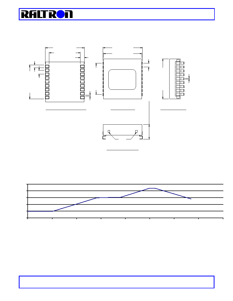
OUTLINE DRAWING
1.040 (26.42 mm)
.840 (21.34 mm)
1.00 (25.40mm)
LABEL
MARKING
FRONT VIEW
.960 (24.38mm)
1.050 (
2
6.
67m
m
)
9
1
.41
6
M
A
X.
(
1
0.57mm
M
A
X
.
PCB FOOTPRINT
.100 (2.54 mm)
.100 (2.
5
4m
m
)
.065 (
1
.
6
5
mm)
.865 (
2
1.
97
mm)
10
18
.035 (
.
89 mm
)
.100 (
.
2.54
mm)
TOP VIEW
SIDE VIEW
.800 (
2
0.32 mm
)
TABS
.
0
1
9
(
.
48
mm)
∑
REFLOW PROFILE
0
50
100
150
200
250
0
1
2
3
4
5
6
7
8
Time (minutes)
Temp (C)