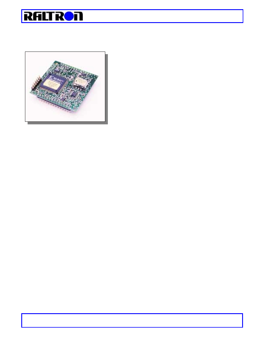
SYNCHRONOUS EQUIPMENT
DUAL OUTPUT HITLESS SWITCHING - SY05-HLPL
RALTRON ELECTRONICS CORP.
!
!
!
!
10651 N.W.19
th
St
!
!
!
!
Florida 33172
!
!
!
!
U.S.A.
Tel: 305 593-6033
!
!
!
!
Fax: 305-594-3973
!
!
!
!
e-mail: sales@raltron.com
!
!
!
!
Internet: http://www.raltron.com
SY05-HLPL
Date: May 20, 2002
�
INTRODUCTION
The SY05-HLPL is a high frequency clock that has been designed to
be use at high speed Line Interface Cards in telecommunication
products mainly related to STN-n or OC-n.
�
FEATURES
A high frequency clock intended to be used at line cards for OC3 and OC12 (STM3 and STM12).
Along with SY0001 or SY05-HLPL provides complete timing solution.
Provides very low jitter output signal from
51.84MHz to 800MHz
Performs hitless switching between two reference signals
Supports four timing modes: (1) Free-run, (2) Locked to Reference 1 (3) Locked to Reference 2, and (4) Loop-
back timing.
Accepts reference inputs from two clock sources from
8kHz to 77.76MHz
Manual or Automatic selection between operating modes.
Alarm and status signals.
Complies with ITU-T Recommendations G.813, ETSI-ETS 300 462-4 and Bellcore GR-1244-CORE for Stratum
3 and 3E applications.
Small dimensions of 1.8 x 1.8 x 0.50 inch.
�
APPLICATION
The SY05-HLPL high frequency clock can be used in ATM, SDH, PDH, and SONET networks devices. It is
designed for manufacturers of network equipment, especially Access Switches, Core Switches, Cross Connects,
Digital Multiplexers-Exchangers, and SDH/SONET equipment. The SY05-HLPL is a timing solution for Line
Interface Cards.

SYNCHRONOUS EQUIPMENT
DUAL OUTPUT HITLESS SWITCHING - SY05-HLPL
RALTRON ELECTRONICS CORP.
!
!
!
!
10651 N.W.19
th
St
!
!
!
!
Florida 33172
!
!
!
!
U.S.A.
Tel: 305 593-6033
!
!
!
!
Fax: 305-594-3973
!
!
!
!
e-mail: sales@raltron.com
!
!
!
!
Internet: http://www.raltron.com
Figure 1. - The functional block diagram of SY05-HLPL
�
DESCRIPTION
The SY05-HLPL synchronization module is a high frequency PLL that performs hitless switching plus additional
features necessary for timing at high-speed Line Interface Cards. The functional block diagram is shown in figure 1.
The SY05-HLPL receives two reference signals, usually 19.44MHz and using PLL synthesizer generates a high
frequency signal necessary for transceivers or framers. The PLL that is complemented by high-speed logic that
provide processing, switching between the timing modes, alarm and status messages and etc. A high quality VCXO
provides very low jitter at the output. The additional output is provided using a divider.
The module supports two operating modes: AUTO mode is the mode where all switching are done automatically
and MANUAL mode is where unit will switch according to the two external control pins CON1 and CON2.
CON1 CON2
Operational
mode
0 0 Free-run
(Unlocked)
1
0
Locked to EX REF 1
0
1
Locked to EX REF 2
1
1
Locked to TLB REF
The module operates in the following four timing modes: 1) Free-run, 2) Locked to EX REF1, 3) Locked to EX REF2
and 4) Locked to TBL REF. Free-run it a mode the unit is unlocked to either of the inputs. The accuracy of the
output frequencies in this mode is equal to the accuracy of free running VCXO. Locked to EX REF 1 is the mode
where the output of the module is phase locked to input reference 1. Locked to EX REF 2 is the mode where the
output of the module is phase locked to input reference 2, Locked to TBL REF is the mode where is the output of
the module is phase locked to the signal used in Time Loop-back operation.
MUX,
COUNTERS
&
CONTROL
LOGIC
PLL
(PD+
LF)
�
�
�
�
OUT
PECL
OPT OUT
PECL
STATUS
SIGNALS
CU#1
STATUS
SIGNALS
CU#2
EX REF1
CNT1 CNT2
TLB REF
ALARM &
STATUS
REV/NONREV
VCXO
EX REF2
AUTO/MAN
SYNCHRONOUS EQUIPMENT
DUAL OUTPUT HITLESS SWITCHING - SY05-HLPL
RALTRON ELECTRONICS CORP.
!
!
!
!
10651 N.W.19
th
St
!
!
!
!
Florida 33172
!
!
!
!
U.S.A.
Tel: 305 593-6033
!
!
!
!
Fax: 305-594-3973
!
!
!
!
e-mail: sales@raltron.com
!
!
!
!
Internet: http://www.raltron.com
�
SPECIFICATIONS
General
Specifications
Mechanical
1.82" (D) x 1.82" (W) x 0.425" (H)
1.95" (D) x 1.95" (W) x 0.45" (H)
Metal Box
Module on PCB
Power
Supply
+3.3VDC
Current Supply
TBD
Operating Temperature
-20�C to 70�C
Storage Temperature
-40� to 85�C
Humidity
5% to 95% non-condensing
Internal Oscillators
VCXO
SAW oscillators
Input Signals
Number of Inputs
2
Input reference frequency
8KHz~19.44MHz
Signal Level
HCMOS/TTL Compatible
Number of Outputs
2
Output 1
155.52MHz
622.08MHz optional
Output 2
Out1 divide by 2/4 or 8
Output Signal
Signal Level
LVPECL
50+/-5%
Signal Quality
Performance
Jitter Tolerance
Bell-core: GR-1244-core 4.2, ITU-T: G.812
Phase Transient Tolerance
Bell-core: GR-1244-core 4.4
Wander Tolerance
Bell-core: GR-1244-core 4.3, ITU-T: G.812
Jitter Generation and Transfer
Bell-core: GR-1244-core 5.5, ITU-T: G.812
Frequency Output
Performance
Free run accuracy
�
20ppm
Pull-In
Range
�
50ppm
MTIE
Bell-core: GR-1244-core 4.2, ITU-T: G.812
TDEV
Bell-core: GR-1244-core 4.2, ITU-T: G.812
SYNCHRONOUS EQUIPMENT
DUAL OUTPUT HITLESS SWITCHING - SY05-HLPL
RALTRON ELECTRONICS CORP.
!
!
!
!
10651 N.W.19
th
St
!
!
!
!
Florida 33172
!
!
!
!
U.S.A.
Tel: 305 593-6033
!
!
!
!
Fax: 305-594-3973
!
!
!
!
e-mail: sales@raltron.com
!
!
!
!
Internet: http://www.raltron.com
�
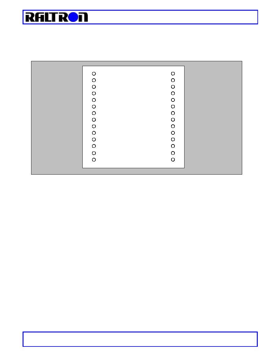
PIN ASSIGNMENT
On the picture below it is shown the pin-out for the SY05-HLPL. For other pin-out requirement please contact the
Raltron.
Figure 3 � Bottom view
1
2
3
4
5
6
7
8
9
10
11
12
13
14
28
27
26
25
24
23
22
21
20
19
18
17
16
15
Vcc
REF1 UL
GND
EX REF 1
REF2 UL
GND
CNT 1
CNT 2
EX REF2
OPT OUT COMP
OPT OUT
REF1 HL
REF2 HL
REF2 AL
GND
TLB OK
TLB REF COMP
TLB REF
GND
REF1 FR
REF2 FR
REF1 AL
REV/NONREV
GND
OUT
OUT COMP
AUTO/MAN
ALARM
SYNCHRONOUS EQUIPMENT
DUAL OUTPUT HITLESS SWITCHING - SY05-HLPL
RALTRON ELECTRONICS CORP.
!
!
!
!
10651 N.W.19
th
St
!
!
!
!
Florida 33172
!
!
!
!
U.S.A.
Tel: 305 593-6033
!
!
!
!
Fax: 305-594-3973
!
!
!
!
e-mail: sales@raltron.com
!
!
!
!
Internet: http://www.raltron.com
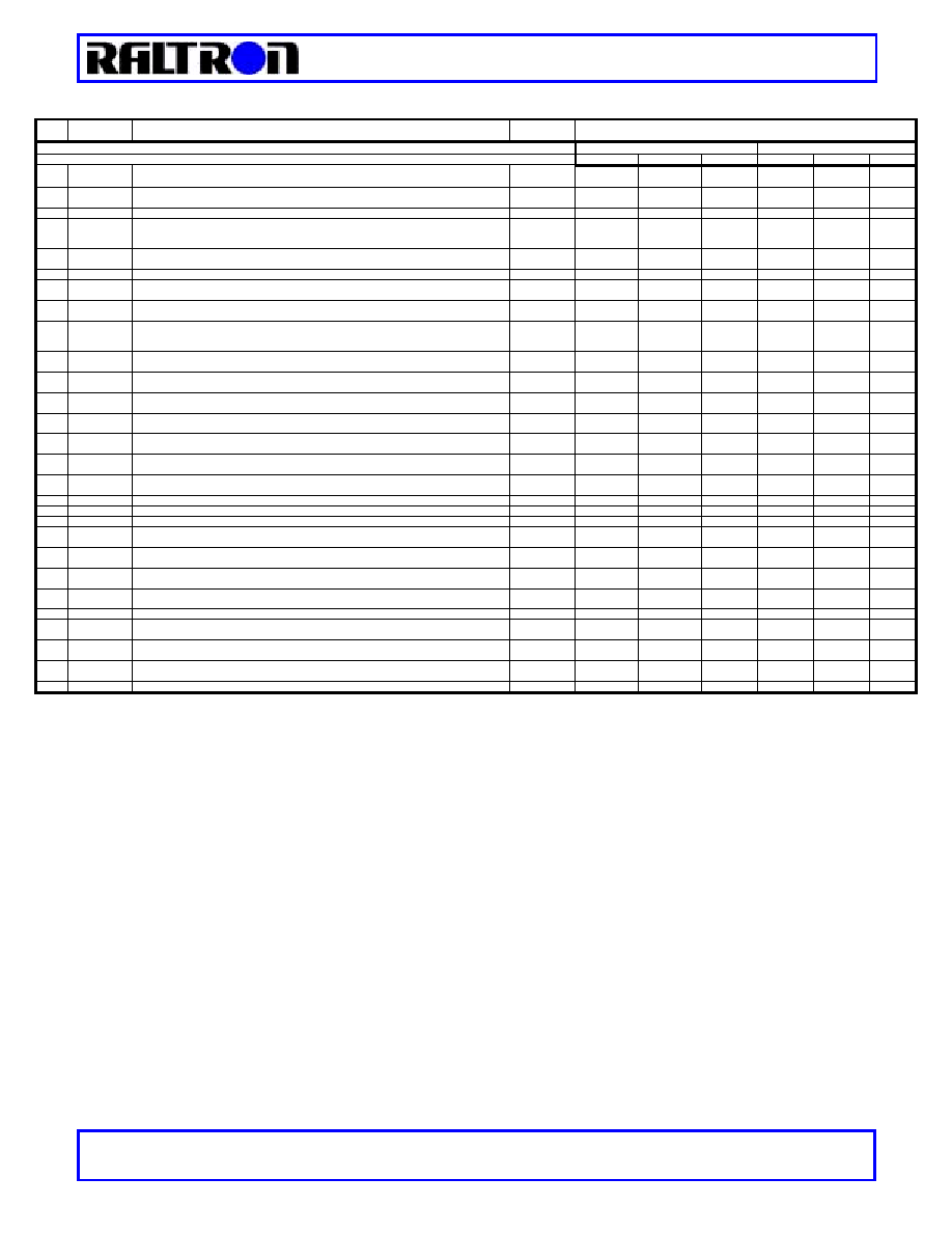
Pin
#
Name Description
Signal
Technology
VL
VH/ DC Voltage
Min Typ
Max
Min
Typ
Max
1 +Vcc
Positive Voltage Supply
DC
----- ----- -----
4.75**
(3.135)
5.0**
(3.3)
5.25**
(3.465)
2
REF1 UL
Reference 1 Unlocked Input -> the signal PLL UNLOCK comes from Clock Unit 1
DC
0 0.25
**
(0.15)
0.5**
(0.3)
4.5**
(2.97)
5.0**
(3.3)
5.25**
(3.465)
3 GND
Ground
----- ----- ----- ----
------
------
------
4
EX REF 1
External Reference 1 Input -> the input signal from reference 1
HCMOS
(3.3
Tolerable)
0
-----
0.5**
(0.3)
4.5** (2.97) ---- ----
5 REF2
UL
Reference 2 Unlocked Input -> the signal PLL UNLOCK comes from Clock Unit 2
DC
0 0.25
**
(0.15)
0.5**
(0.3)
4.5**
(2.97)
5.0**
(3.3)
5.25**
(3.465)
6 GND
Ground
----- ----- ----- ----
------
------
------
7 CNT
2
Control Input 2 -> the external input for selecting mode of the unit � see table.
DC
0
0.25 (0.15)
0.5
(0.3)
4.5
(2.97)
5.0
(3.3)
5.25
(3.465)
8 CNT
1
Control Input 1 -> the external input for selecting mode of the unit � see table.
DC
0 0.25
**
(0.15)
0.5**
(0.3)
4.5**
(2.97)
5.0**
(3.3)
5.25**
(3.465)
9
EX REF 2
External Reference 2 Input -> the input signal from reference 2
HCMOS
(3.3
Tolerable)
0
-----
0.5**
(0.3)
4.5** (2.97) ---- ----
10
OPT OUT
COMP
Optional Output -> the secondary output of the synchronized signal, for frequency range see
table below
LV/PECL Vcc-1.680 Vcc-1.620 Vcc-1.560 Vcc-1.085 Vcc-1.025 Vcc-0.885
11 OPT
OUT
Optional Output -> the secondary output of the synchronized signal, for frequency range see
table below.
LV/PECL Vcc-1.680 Vcc-1.620 Vcc-1.560 Vcc-1.085 Vcc-1.025 Vcc-0.885
12 REF1
HL
Reference 1 Holdover Input -> the signal HOLDOVER comes from Clock Unit 1
DC
0 0.25
**
(0.15)
0.5**
(0.3)
4.5**
(2.97)
5.0**
(3.3)
5.25**
(3.465)
13 REF2
HL
Reference 2 Holdover Input -> the signal HOLDOVER comes from Clock Unit 2
DC
0 0.25
**
(0.15)
0.5**
(0.3)
4.5**
(2.97)
5.0**
(3.3)
5.25**
(3.465)
14 REF2
AL
Reference 2 Alarm Input -> the signal ALARM OUT comes from Clock Unit 2
DC
0 0.25
**
(0.15)
0.5**
(0.3)
4.5**
(2.97)
5.0**
(3.3)
5.25**
(3.465)
15 ALARM
Alarm signal -> the output is high when there is an alarm in the module
DC
0 0.25
**
(0.15)
0.5**
(0.3)
4.5**
(2.97)
5.0**
(3.3)
5.25**
(3.465)
16 AUTO/MAN
Auto/Manual configuration input -> selection input for operating mode
DC
0 0.25
**
(0.15)
0.5**
(0.3)
4.5**
(2.97)
5.0**
(3.3)
5.25**
(3.465)
17
OUT
Synchronized Output -> the output of the synchronized signal.
LV/PECL
Vcc-1.680
Vcc-1.620
Vcc-1.560
Vcc-1.085
Vcc-1.025
Vcc-0.885
18
OUT COMP
Synchronized Complementary Output -> the output of the synchronized signal.
LV/PECL
Vcc-1.680
Vcc-1.620
Vcc-1.560
Vcc-1.085 Vcc-1.025 Vcc-0.885
19 GND Ground
----- ----- ----- ----
------
------
------
20 RV/NRV
Revert / Non revert input-> selection input for revert feature
Revertive-"1" ; Non-Revertive = "0"
DC
0 0.25
**
(0.15)
0.5**
(0.3)
4.5**
(2.97)
5.0**
(3.3)
5.25**
(3.465)
21 REF1
AL
Reference 1 Alarm Input -> the signal ALARM OUT comes from Clock Unit 1
DC
0 0.25
**
(0.15)
0.5**
(0.3)
4.5**
(2.97)
5.0**
(3.3)
5.25**
(3.465)
22 REF2
FR
Reference 2 Free-run Input -> the signal FREERUN comes from Clock Unit 2
DC
0 0.25
**
(0.15)
0.5**
(0.3)
4.5**
(2.97)
5.0**
(3.3)
5.25**
(3.465)
23 REF1
FR
Reference 1 Free-run Input -> the signal FREERUN comes from Clock Unit 1
DC
0 0.25
**
(0.15)
0.5**
(0.3)
4.5**
(2.97)
5.0**
(3.3)
5.25**
(3.465)
24 GND Ground
----- ----- ----- ----
------
------
------
25 TLB
REF
Time Loop-back Reference Input -> the input from time loop-back reference
DC
0 0
0.25
**
(0.15)
0.5**
(0.3)
4.5**
(2.97)
5.0**
(3.3)
26
TLB REF
COMP
Time Loop-back Reference Complementary Input -> the input from time loop-back
DC
0 0
0.25
**
(0.15)
0.5**
(0.3)
4.5**
(2.97)
5.0**
(3.3)
27 TLB
OK
Time Loop-back OK -> The reference is valid for use.
DC
0 0.25
**
(0.15)
0.5**
(0.3)
4.5**
(2.97)
5.0**
(3.3)
5.25**
(3.465)
28 GND Ground
----- ----- ----- ----
------
------
------