This product conforms to specifications per the terms of the Ramtron
Ramtron International Corporation
standard warranty. Production processing does not necessarily in-
1850 Ramtron Drive, Colorado Springs, CO 80921
clude testing of all parameters.
(800) 545-FRAM, (719) 481-7000, Fax (719) 481-7058
www.ramtron.com
Rev 2.1
Dec. 2002
Page 1 of 18
FM30C256
256Kb Data Collector
Features
256K bit Ferroelectric Nonvolatile RAM
∑
Organized as 32,768 x 8 bits
∑
High Endurance 10 Billion (10
10
) Read/Writes
∑
10 year Data Retention
∑
NoDelayTM Writes
∑
Advanced High-Reliability Ferroelectric Process
Fast Two-wire Serial Interface
∑
Up to 1 MHz Maximum Bus Frequency
∑
Supports Legacy Timing for 100 kHz & 400 kHz
∑
Clock Registers Accessed via 2-wire Interface
Real-time Clock/Calendar
∑
Backup Current under 1
µ
A
∑
Tracks Seconds through Centuries (BCD format)
∑
Tracks Leap Years through 2099
∑
Uses Standard 32.768 kHz Crystal (6pF)
∑
Software Calibration
System Supervisor
∑
Active-low Reset Output for V
DD
Out-of-Tolerance
∑
Tamper Detect Input with Battery Backup and
Time Stamp
Description
The FM30C256 is a 256-kilobit data collection
subsystem including nonvolatile RAM, timekeeping,
CPU supervisor, and system tamper detection. Non-
volatile RAM is provided by FRAM technology,
which is ideal for collection data and requires no
battery backup for nonvolatile storage. In other
respects, it provides the same features as SRAM.
FRAM performs write operations at bus speed with
no write delays. Write cycles can be continuous
without block limitations. In addition, it offers much
higher write endurance than other nonvolatile
memories. The FM30C256 supports up to 10
10
read/write cycles.
The FM30C256 also includes timekeeping with
external battery backup. The timekeeper consists of
registers that represent time and date information in
BCD format. The clock includes a calibration mode
that allows a software adjustment for timekeeping
accuracy.
To maintain system data integrity, the FM30C256
provides a reset signal asserted when VDD is out of
tolerance. /RST remains active for 100 ms after VDD
returns to proper levels. The FM30C256 also
provides a battery-backed tamper detect circuit that
records a rising edge on the TIN input. A battery-
backed flag is set when the event occurs, but can only
be cleared by software.
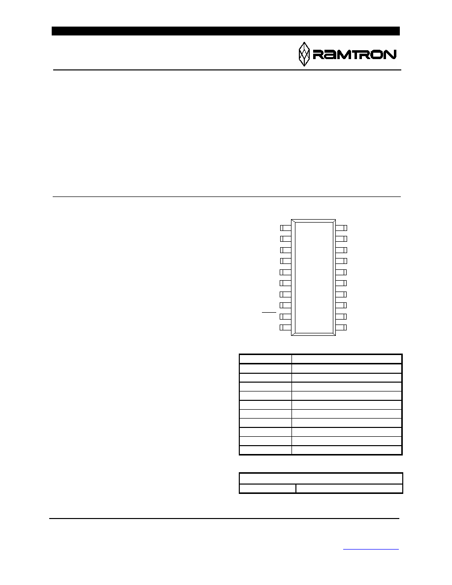
The FM30C256 is provided in a 20-pin SOIC
package and is guaranteed over an industrial
temperature range of ≠40∞C to +85∞C.
Pin Configuration
Pin Names
Function
TIN
Tamper Detect input
A0-A2 Device
Select
inputs
CAL
Clock Calibration output
/RST Reset
Output
X1, X2
Crystal Connections
SDA Serial
Data
SCL Serial
Clock
VDD Supply
Voltage
5V
VBAK Battery-Backup
input
VSS Ground
Ordering Information
FM30C256-S 20-pin
SOIC
VDD
VBAK
SCL
SDA
VSS
X1
X2
CAL
TIN
NC
NC
NC
NC
RST
NC
A0
A1
A2
NC
NC
1
2
3
4
5
6
7
8
9
10
20
19
18
17
16
15
14
13
12
11
FM30C256
Rev 2.1
Dec. 2002
Page 2 of 18
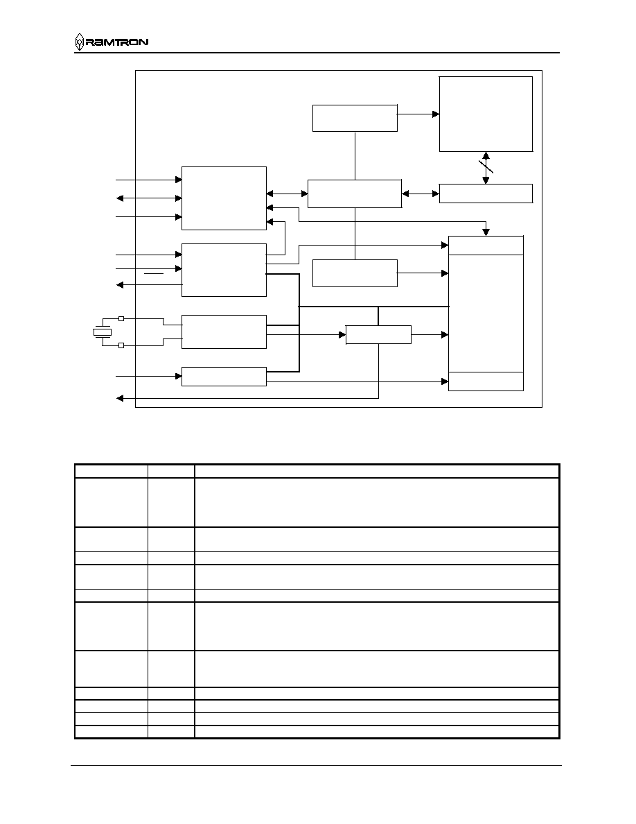
Figure 1. Block Diagram
Pin Descriptions
Pin Name
Type
Pin Description
A2-A0
Input
Device select inputs are used to address the part on a serial bus. To select the device,
the address value on the three pins must match the corresponding bits contained in
the device address. Note that these are not address pins for read/write operations.
The address pins are pulled down internally.
TIN
Input
Tamper detect is a battery backed input that stores a 1 in the Flags/Control register
when it detects a rising edge on the TIN pin.
CAL
Output
512 Hz square-wave output for clock calibration
X1, X2
I/O
32.768 kHz crystal connection. When using an external oscillator source, use X2 as
the oscillator input and leave X1 floating.
/RST
Output
Active low reset output (open drain)
SDA
I/O
Serial Data Address. This is a bi-directional line for the two-wire interface. It is
open-drain and is intended to be wire-OR'd with other devices on the two-wire bus.
The input buffer incorporates a Schmitt trigger for noise immunity and the output
driver includes slope control for falling edges. A pull-up resistor is required.
SCL
Input
Serial Clock. The serial clock line for the two-wire interface. Data is clocked out of
the part on the falling edge, and in on the rising edge. The SCL input also
incorporates a Schmitt trigger input for noise immunity.
VBAK
Supply
Battery backup supply voltage (3V)
VDD Supply
Supply
Voltage
(5V)
VSS Supply
Ground
NC -
No
connect
Address Latch &
Counter
32K x 8
FRAM Array
RTC Address
Latch & Counter
Serial to Parallel
Converter
Data Latch
8
Protocol &
Device Select
Real-time Clock
Registers
Power Isolation
Tamper Flag
Counters
Power
Management
RTC Oscillator
Tamper Latch
Battery-backed power
CAL
TIN
X2
X1
RST
VBAK
VDD
SCL
SDA
A2-A0
32.768
kHz
FM30C256
Rev 2.1
Dec. 2002
Page 3 of 18
Overview
The FM30C256 data collector combines a 256Kb
serial nonvolatile RAM with a real-time clock (RTC),
a power monitor, and a tamper detect circuit. The
FM30C256 integrates these complementary but
distinct functions under a common interface in a
single package. Despite providing multiple interface
Ids as explained below, the product is a single
monolithic device.
The memory is organized as 32Kx8 of FRAM and is
accessed via a separate 2-wire device ID from the
remaining functions. This allows the user to preserve
addressing information when switching between
memory and RTC functions. Modularity in software
design is preserved as well.
The real-time clock function and the tamper detection
is accessed under its own 2-wire device ID. This
allows clock data to be read while maintaining the
last (most recently used) memory address in the other
device. The clock and tamper functions are controlled
by 9 registers that are backed up by the external
battery. Clock and tamper functions continue to
operate from battery power when V
DD
drops below
the battery voltage.
In addition to the software-controlled functions, the
FM30C256 also provides reset signal for an external
microcontroller host. This signal is asserted when
V
DD
drops below the specified trip point (V
TP
). It
remains asserted until V
DD
returns above V
TP
for the
hold-off period (t
RPU
). The power monitor has no
interaction with other software-controlled functions.
Any access to the device will be ignored when V
DD
<
V
TP
.
Memory Operation
When accessing the FM30C256, the user addresses
32,768 locations each with 8 data bits. These data bits
are shifted in and out serially. The 32,768 addresses
are accessed using the two-wire protocol, which
includes a slave address (to distinguish from other
non-memory devices), and an extended 16-bit
address. The decoder uses only the lower 15 bits for
accessing the memory. The upper address bit should
be set to 0 for compatibility with larger devices in the
future.
The memory is read or written at the speed of the
two-wire bus. The interface protocol is described
further below.
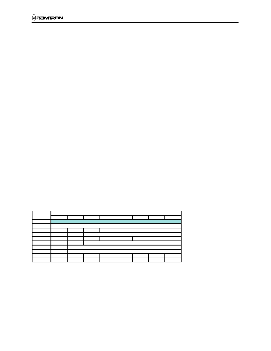
RTC Register Map
The interface to clock and tamper functions is via 9
address locations mapped to a separate 2-wire device
ID. The interface protocol is described below. The
registers contain timekeeping data, control bits, or
information flags. A short description of each register
follows. Detailed descriptions follow the register
summary section.
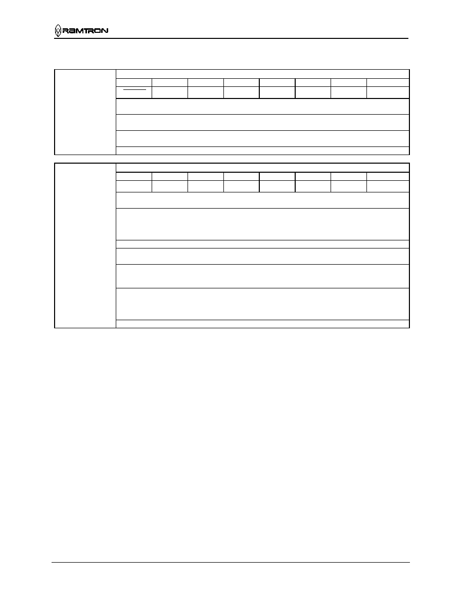
Register Map Summary Table
Data
Address
D7
D6
D5
D4
D3
D2
D1
D0
Function
Range
9-F
8
10 years
years
Years
00-99
7
0
0
0
10 mo
months
Month
1-12
6
0
0
10 date
date
Date
1-31
5
0
0
0
0
0
day
Day
1-7
4
0
0
10 hours
hours
Hours
0-23
3
0
10 minutes
minutes
Minutes
0-59
2
0
10 seconds
seconds
Seconds
0-59
1
/OSCEN
TSEN
CALS
CAL4
CAL3
CAL2
CAL1
CAL0
CAL/Control
0
Tamper
CF
reserved reserved
TST
CAL
W
R
Flags/Control
ILLEGAL ADDRESSES
FM30C256
Rev 2.1
Dec. 2002
Page 4 of 18
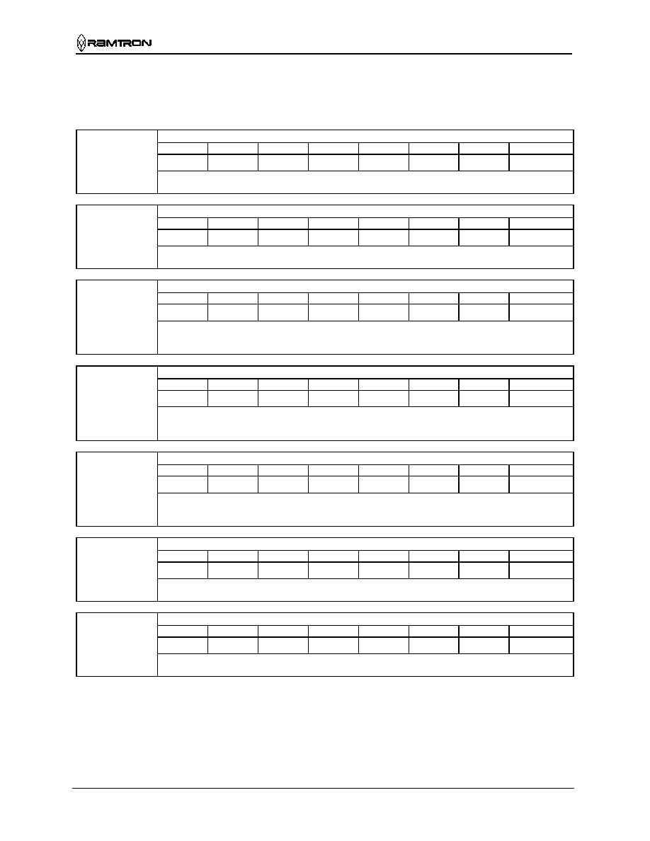
Table 1. Register Map
Address Description
8h
Timekeeping ≠ Years
D7 D6 D5 D4 D3 D2 D1 D0
10 year.3
10 year.2
10 year.1
10 year.0 Year.3 Year.2 Year.1
Year.0
Contains the lower two BCD digits of the year. Lower nibble contains the value for years; upper nibble
contains the value for 10s of years. Each nibble operates from 0 to 9. The range for the register is 0-99.
7h
Timekeeping ≠ Months
D7 D6 D5 D4 D3 D2 D1 D0
0 0 0
10
Month
Month.3
Month.2
Month.1
Month.0
Contains the BCD digits for the month. Lower nibble contains the lower digit and operates from 0 to 9;
upper nibble (one bit) contains the upper digit and operates from 0 to 1. The range for the register is 1-12.
6h
Timekeeping ≠ Date of the month
D7 D6 D5 D4 D3 D2 D1 D0
0
0
10 date.1
10 date.0
Date.3
Date.2
Date.1
Date.0
Contains the BCD digits for the date of the month. Lower nibble contains the lower digit and operates
from 0 to 9; upper nibble contains the upper digit and operates from 0 to 3. The range for the register is 1-
31.
5h
Timekeeping ≠ Day of the week
D7 D6 D5 D4 D3 D2 D1 D0
0 0 0 0 0
Day.2
Day.1
Day.0
Lower nibble contains a value that correlates to day of the week. Day of the week is a ring counter that
counts from 1 to 7 then returns to 1. The user must assign meaning to the day value, as the day is not
integrated with the date.
4h
Timekeeping ≠ Hours
D7 D6 D5 D4 D3 D2 D1 D0
0
0
10 hours.1
10 hours.0
Hours.3
Hours2
Hours.1
Hours.0
Contains the BCD value of hours in 24-hour format. Lower nibble contains the lower digit and operates
from 0 to 9; upper nibble (two bits) contains the upper digit and operates from 0 to 2. The range for the
register is 0-23.
3h
Timekeeping ≠ Minutes
D7 D6 D5 D4 D3 D2 D1 D0
0
10 min.2
10 min.1
10 min.0
Min.3
Min.2
Min.1
Min.0
Contains the BCD value of minutes. Lower nibble contains the lower digit and operates from 0 to 9;
upper nibble contains the upper minutes digit and operates from 0 to 5. The range for the register is 0-59.
2h
Timekeeping ≠ Seconds
D7 D6 D5 D4 D3 D2 D1 D0
0
10 sec.2
10 sec.1
10 sec.0
Seconds.3
Seconds.2
Seconds.1
Seconds.0
Contains the BCD value of seconds. Lower nibble contains the lower digit and operates from 0 to 9;
upper nibble contains the upper digit and operates from 0 to 5. The range for the register is 0-59.
FM30C256
Rev 2.1
Dec. 2002
Page 5 of 18
Address Description
1h
CAL/Control
D7 D6 D5 D4 D3 D2 D1 D0
OSCEN TSEN CALS CAL.4 CAL.3 CAL.2 CAL.1 CAL.0
/OSCEN
/Oscillator Enable. When set to 1, the oscillator is halted. When set to 0, the oscillator runs. Disabling
the oscillator can save battery power during storage. On a power-up without battery, this bit is set to 1.
TSEN
Time Stamp Enable. When set to 1, a Tamper Detect event will record the date and time of the event.
On a power-up without battery, this bit is set to 0.
CALS
Calibration sign. Determines if the calibration adjustment is applied as an addition to or as a subtraction
from the time-base. Calibration is explained below.
CAL.4-0
These five bits control the calibration of the clock.
0h
Flags/Control
D7 D6 D5 D4 D3 D2 D1 D0
Tamper CF Reserved
Reserved
TST CAL W
R
Tamper
Tamper Detect. This bit is set to 1 when rising edge is detected on the TIN pin. It can only be cleared to
0 by the user.
CF
Century Overflow Flag. This bit is set to a 1 when the values in the years register overflows from 99 to
00. This indicates a new century, such as going from 1999 to 2000 or 2099 to 2100. The user should
record the new century information as needed. This bit is cleared to 0 when the Flag register is read. It is
read-only for the user.
TST
Invokes factory test mode. Users should always set this bit to 0.
CAL
Calibration Mode. When set to 1, the clock enters calibration mode. When CAL is set to 0, the clock
operates normally, and the CAL pin is driven low.
W
Write Time. Setting the W bit to 1 freezes updates of the timekeeping registers. The user can then write
them with updated values. Setting the W bit to 0 causes the contents of the time registers to be
transferred to the timekeeping counters.
R
Read Time. Setting the R bit to 1 copies a static image of the timekeeping registers and places them in a
holding register. The user can then read them without concerns over changing values causing system
errors. The R bit going from 0 to 1 causes the timekeeping capture, so the bit must be returned to 0 prior
to reading again.
Reserved
Reserved bits. Do not use. Should remain set to 0.
Real-time Clock Operation
The real-time clock (RTC) consists of an oscillator,
divider, and a register system for accessing the
information. It divides down the 32.768 kHz time-
base and provides a minimum resolution of seconds
(1Hz) to the user. Static registers provide the user
with read/write access to the time values. The
synchronization of these registers with the
timekeeper core is performed using R and W bits in
register 0.
Changing the R bit from 0 to 1 causes a transfer of
the timekeeping information to holding registers that
can be read by the user. If a timekeeper update is
pending when R is set, then the update will be
completed prior to loading the registers. Another
update cannot be performed until the R bit is cleared
to 0.
Setting the W bit to 1 causes the timekeeper to freeze
updates. Clearing it to 0 causes the values in the time
registers to be written into the timekeeper core. Users
should be certain not to load invalid values, such as
FFh, to the timekeeping registers.
Updates to the timekeeping core occur continuously
except when frozen. A diagram of the timekeeping
core follows.
Backup Power
The real-time clock/calendar is intended for
permanently powered operation. When the primary
system power fails, the voltage on the VDD pin will
drop. When VDD is less than the voltage on the
VBAK pin, the clock will switch to the backup power
supply. The clock operates at extremely low current
in order to maximize battery life. However, an
advantage of combining a clock function with FRAM
is that the 256K memory data is not lost regardless of
the backup power source.