 | –≠–ª–µ–∫—Ç—Ä–æ–Ω–Ω—ã–π –∫–æ–º–ø–æ–Ω–µ–Ω—Ç: RC2207N | –°–∫–∞—á–∞—Ç—å:  PDF PDF  ZIP ZIP |

Electronics
Semiconductor Division
Features
∑ Excellent temperature stability -- 20 ppm/
∞
C
∑ Linear frequency sweep
∑ Adjustable duty cycle -- 0.1% to 99.9%
∑ Two or four level FSK capability
∑ Wide sweep range -- 1000:1 min.
∑ Logic compatible input and output levels
∑ Wide supply voltage range --
±
4V to
±
13V
∑ Low supply sensitivity
±
0.15%/V
∑ Wide frequency range -- 0.01 Hz to 1 MHz
∑ Simultaneous triangle and squarewave outputs
Applications
∑ FSK generation
∑ Voltage and current-to-frequency conversion
∑ Stable phase-locked loop
∑ Waveform generation triangle, sawtooth, pulse,
squarewave
∑ FM and sweep generation
Description
The RC2207 is a monolithic voltage-controlled oscillator
(VCO) integrated circuit featuring excellent frequency
stability and a wide tuning range. The circuit provides
simultaneous triangle and squarewave outputs over a
frequency range of 0.01 Hz to 1 MHz. It is ideally suited for
FM, FSK and sweep or tone generation as well as for
phase-locked loop applications.
As shown in the Block Diagram, the circuit is comprised of
four functional blocks: a variable-frequency oscillator which
generates the basic periodic waveforms; four current
switches actuated by binary keying inputs; and buffer
amplifiers for both the triangle and squarewave outputs.
The internal switches transfer the oscillator current to any
of four external timing resistors to produce four discrete
frequencies which are selected according to the binary logic
levels at the keying terminals (pins 8 and 9).
The RC2207 has a typical drift specification of 20 ppm/
∞
C.
The oscillator frequency can be linearly swept over a 1000:1
range with an external control voltage; and the duty cycle of
both the triangle and the squarewave outputs can be varied
from 0.1% to 99.9% to generate stable pulse and sawtooth
waveforms.
RC2207
Voltage Controlled Oscillator
Rev. 1.0.0
Block Diagram
A1
A2
VCO
TIMING CAPACITOR
TIMING RESISTORS
R1-R4
CURRENT
SWITCH
TRIANGLE WAVE OUTPUT
BINARY KEY INPUTS
SQUARE WAVE OUTPUT
≠V
S
65-2207-01
RC2207
PRODUCT SPECIFICATION
2
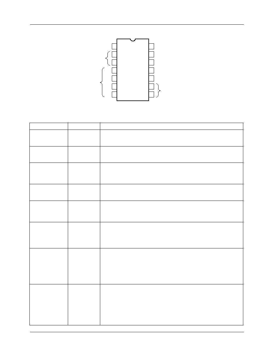
Pin Assignments
Pin Descriptions
Pin Name
Pin Number
Pin Function Description
Bias for Single
Supply
11
For single supply operations, pin 11 should be externally biased to a
potential between +V
S
/3 and +V
S
/2 (see Figure 8). The bias current at pin
11 is nominally 5% of the total oscillation timing current I
T
.
Binary Keying
Inputs
8, 9
The internal impedance at these pins is approximately 5 k
. Keying levels
are <1.4V for zero and > 3V for one logic levels referenced to the DC voltage
at pin 10.
Ground
10
For split supply operation, this pin serves as circuit ground. For single supply
operation, pin 10 should be AC grounded through a 1
µ
F bypass capacitor.
During split supply operation, a ground current of 2 I
T
flows out of this
terminal, where I
T
is the total timing current.
Squarewave
Output
13
The squarewave output at pin 13 is an open-collector stage capable of
sinking up to 20 mA of load current. R
L
serves as a pull-up load resistor for
this output. Recommended values for R
L
range from 1 k
to 10 k
Supply Voltage
(+V
S
, ≠V
S
)
1, 12
The RC2207 is designed to operate over a power supply range of +4V to
±
13V for split supplies, or 8V to 26V for single supplies. At high supply
voltages, the frequency sweep range is reduced. Performance is optimum
for
±
6V, or 12V single supply operation.
Timing Capacitor
2, 3
The oscillator frequency is inversely proportional to the timing capacitor, C.
The minimum capacitance value is limited by stray capacitances and the
maximum value by physical size and leakage current considerations.
Recommended values range from 100 pF to 100
µ
F. The capacitor should
be non-polarized.
Timing Resistors
(R1≠R4)
4≠7
The timing resistors determine the total timing current, I
T
, available to
charge the timing capacitor. Values for timing resistors can range from 1.5
k
to 2 M
; however, for optimum temperature and power supply stability,
recommended values are 4 k
to 200 k
. To avoid parasitic pick up, timing
resistor leads should be kept as short as possible. For noise environments,
unused or deactivated timing terminals should be bypassed to ground
through 0.1
µ
F capacitors. Otherwise, they may be left open.
Trianglewave
Output
14
The output at pin 14 is a trianglewave with a peak swing of approximately
one-half of the total supply voltage. Pin 14 has a very low output impedance
of 10
and is internally protected against short circuits.
Notice that the triangle waveform linearity is sensitive to parasite coupling
between the square and the trianglewave outputs (pins 13 and 14). In board
layout or circuit wiring, care should be taken to minimize stray wiring
capacitance between those pins.
1
2
3
4
5
6
7
14
13
12
11
10
9
8
65-2207-02
Binary
Keying
Inputs
GND
Bias
Squarewave Output
Trianglewave Output
+V
S
Timing
Capacitor
Timing
Resistors
R1
R2
R3
R4
+V
S

PRODUCT SPECIFICATION
RC2207
3
Absolute Maximum Ratings
Thermal Characteristics
Parameter
Min.
Max.
Units
Supply Voltage
+26
V
Storage Temperature Range
-65
+150
V
Operating Temperature Range
-55
+125
∞
C
Lead Soldering Temperature (60 seconds)
+300
∞
C
Ceramic DIP
SOIC
Plastic DIP
Maximum Juncton Temperature
+175
∞
C
+125
∞
C
+125
∞
C
Maximum P
D
T
A
< 50
∞
C
1042 mW
300 mW
468 mW
Thermal Resistance,
JC
60
∞
C/W
60
∞
C/W
60
∞
C/W
Thermal Resistance,
JA
120
∞
C/W
200
∞
C/W
160
∞
C/W
For T
A
> 50
∞
C Derate at
8.33 mW/
∞
C
5.0 mW/
∞
C
6.25 mW/
∞
C

RC2207
PRODUCT SPECIFICATION
4
Electrical Characteristics
(Test Circuit of Figure 1, V
S
=
±
6V, T
A
= +25
∞
C, C = 5000 pF, R1= R2 = R3 = R4 = 20 k
, R
L
= 4.7
binary inputs
grounded, S1 and S2 closed unless otherwise specified)
Note:
1. Guaranteed by design.
Parameters
Test Conditions
Min.
Typ.
Max.
Units
General Characteristics
Supply Voltage
Single Supply
See Typical Performance
Characteristics
+8.0
+12
+26
V
Split Supplies
±
4
±
6
±
13
V
Supply Current
Single Supply
Measured at pin 1,
S1 open (See Fig. 8)
5.0
7.0
mA
Split
Supplies
Positive
Measured at pin 1,
S1 open (See Fig. 7)
RC2207
5.0
7.0
mA
RM2207
8.0
Negative
Measured at pin 12,
S1, S2 open
RC2207
7.0
mA
RM2207
4.0
6.0
Binary Keying Inputs
Switching Threshold
Measured at pins 8 and 9.
Refer to pin 10.
1.4
2.2
2.8
V
Input Resistance
5.0
k
Oscillator Section--Frequency Characteristics
Upper Frequency Limit
C = 500 pF, R3 = 2 k
0.5
1.0
MHz
Lower Practical Frequency
C = 50
µ
F, R3 = 2 k
0.01
Hz
Frequency Accuracy
±
1.0
±
3.0
% of f
0
Frequency Matching
0.5
% of f
0
Frequency
Stability
vs. Temperature (Note 1)
0
∞
C < T
A
< +70
∞
C
20
50
ppm/
∞
C
vs. Supply Voltage
0.15
%/V
Sweep Range
R3 = 1.5 k
for f
H
R3 = 2 M
for f
L
1000:1
3000:1
f
H
/f
L
Sweep Linearity
C = 5000 pF
10:1 Sweep
1
f
H
= 10 kHz, f
L
= 1 kHz
1.0
2.0
%
1000:1 Sweep
f
H
= 100 kHz, f
L
= 100 Hz
5.0
%
FM Distortion
±
10% FM Deviation
0.1
%
Recommended Range of Timing Resistors
See Characteristic Curves
1.5
2000
k
Impedance at Timing Pins
Measured at pins 4, 5, 6, or 7
75
DC Level at Timing Terminals
10
mV
Output Characteristics
Triangle output
Amplitude
Measured at pin 14
4
6
V
P-P
Impedance
10
DC Level
Referenced to pin 10
+100
mV
Linearity
from 10% to 90% of swing
0.1
%
Squarewave
Output
Amplitude
Measured at pin 13,
S2 Closed
11
12
V
P-P
Saturation Voltage
Referenced to pin 12
0.2
0.4
V
Rise Time
C
L
10 pF
200
ns
Fall Time
C
L
10 pF
20
ns
PRODUCT SPECIFICATION
RC2207
5
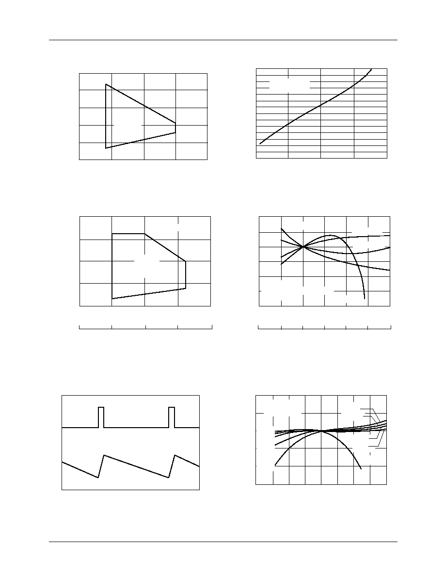
Typical Performance Characteristics
Figure 1. Typical Operating Range for
Figure 2. Frequency Accuracy vs. Timing Resistance
Split Supply Voltage
Figure 3. Recommended Timing Resistor Value vs.
Figure 4. Normalized Frequency Drift vs.
Power Supply Voltage
Supply Voltage
Figure 5. Pulse and Sawtooth Outputs
Figure 6. Normalized Frequency Drift vs. Temperature
,,,,,,,
,,,,,,,
,,,,,,,
,,,,,,,
,,,,,,,
,,,,,,,
,,,,,,,
,,,,,,,
,,,,,,,
,,,,,,,
65-2207-03
Typical
Operating
Range
+25
+20
+15
+10
+5
0
0
-5
-10
-15
-20
Negative Supply (V)
Positive Supply (V)
65-2207-04
V
S
= +6V
C = 5000 pF
7
6
5
4
3
2
1
0
-1
-2
-3
-4
-5
-6
-7
1K
10K
100K
1M
10M
Timing Resistance (
)
Frequency Accuracy (% Error)
,,,,,,,,
,,,,,,,,
,,,,,,,,
,,,,,,,,
,,,,,,,,
,,,,,,,,
,,,,,,,,
,,,,,,,,
,,,,,,,,
,,,,,,,,
Timing
Resistor
Range
T
A
= +25
∞
C
Total Timing Resistor (
)
Split Supply Voltage (V)
Single Supply Voltage (V)
65-2207-05
0
4
8
12
16
0
8
16
24
32
10M
1M
100K
10K
1K
1
R
T
= Parallel Combination of Activated Timing Resistors
Normalized Frequency Drift
Split Supply Voltage (V)
Single Supply Voltage (V)
65-2207-06
2
1.04
1.02
1.00
0.98
0.96
0.94
0.92
4
8
6
10
12
14
4
8
14
12
18
20
22
R
T
= 2 M
R
T
= 20 k
R
T
= 200 k
R
T
= 2 k
T
A
= +20
∞
C
R
T
= Total Timing Resistance
C = 5000 pF
65-2207-07
-50
-75
0
-25
+25
+75
+50
+125
+100
65-2207-08
Temperature (
∞
C)
Normalized Frequency Drift (%)
+2
+1
0
-1
-2
-3
V
S
= +6V
C = 5000 pF
2 M
200 k
2 k
4 k
R = 2 k
4 k
2 k
20 k
200 k
2 M