 | –≠–ª–µ–∫—Ç—Ä–æ–Ω–Ω—ã–π –∫–æ–º–ø–æ–Ω–µ–Ω—Ç: RC5033M | –°–∫–∞—á–∞—Ç—å:  PDF PDF  ZIP ZIP |
Electronics
Semiconductor Division
PRELIMINARY INFORMATION
describes products that are not in full production at the time of printing. Specifications are based on design goals
and limited characterization. They may change without notice. Contact Raytheon for current information.
Pr
eliminar
y Infor
mation
Features
∑ >85% Efficiency
∑ 350uA quiescent current in shutdown
∑ Fast transient response
∑ Soft control power-up
∑ Over-Voltage Protection
∑ Output voltage range from 2.0V to 3.6V
∑ Factory trimmed low TC reference voltage
∑ Adjustable oscillator frequency
∑ Drives N-Channel MOSFETs
∑ 16 pin SOIC package
Applications
∑ 3.3V power supply for PentiumTM based CPU
motherboards
∑ 3.45V power supply for AMD-K5TM CPU
∑ 2.5V or 3.6V power supply for PowerPCTM
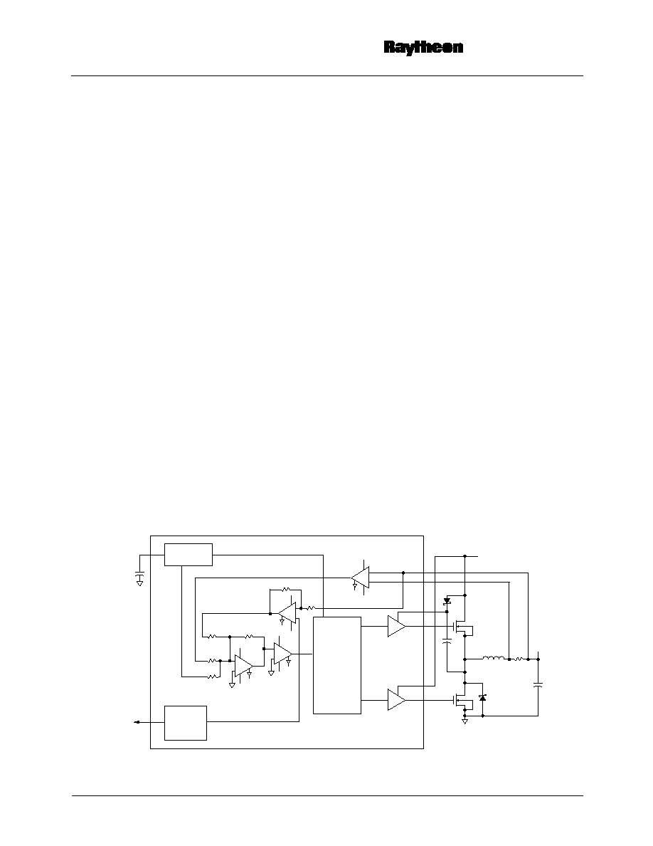
Description
The RC5033 is a synchronous mode DC-DC controller IC
dedicated to providing a 5V to 2.0V up to 3.6V conversion
for various types of CPU power . It can be configured in both
the synchronous and non-synchronous modes and with the
proper applications circuitry can be used to deliver load cur-
rent greater than 10 Amps. The RC5033 is designed to oper-
ate in a standard PWM control mode under heavy load
conditions and as a PFM controller in light load conditions.
Its highly accurate low TC reference eliminates the need for
precision external components in order to achieve tight
tolerance voltage regulation. Through the use of external
resistors, the RC5033 can generate accurate output voltages
from 2.0V up to 3.6V. An integrated Over-Voltage protection
function constantly monitors the output voltage and shuts
down the power to the CPU in the event of a out-of-
tolerance voltage situation, thereby protecting the CPU.
The programmable oscillator can operate from 200KHz to
greater than 1MHz to provide for flexibility in choosing
external components such as inductors, capacitors, and
Power MOSFETs.
Block Diagram
DIGITAL
CONTROL
≠
+
+
≠
I
VREF
65-5033-01
OSC
VREF
≠
+
+
≠
I
≠
+
+
≠
I
≠
+
+
≠
I
VIN
VO
RC5033
Adjustable Synchronous DC-DC Converter
Rev. 0.9.5

PRODUCT SPECIFICATION
RC5033
2
Pr
eliminar
y Infor
mation
Pin Assignments
Pin Definitions
Note:
1. See voltage adjust table for function
Output Voltage Selection Table
Note:
1. See Figure 3 for resistor connection.
2. Indicated short pins together.
Pin Name
Pin Number
Pin Function Description
On/Off
1
A low level on this pin will power down; tie to VCCD if not used.
IFB
2
Current Feedback Input.
VFB
3
Voltage Feedback Input.
VCCA
4
Analog VCC.
VCCD
5
Digital VCC.
VCCP
6
VCC for synchronous FET output drivers.
LODRV
7
Synchronous FET driver output.
GNDP
8
Power ground for high current drivers.
HIDRV
9
High side FET driver output.
VCCQP
10
VCC for High side FET output driver
ADJ1
11
VREF adjust pin.
1
ADJ2
12
VREF adjust pin.
1
GNDD
13
Digital ground.
ADJ3
14
VREF adjust pin.
1
GNDA
15
Analog ground.
CEXT
16
External capacitor for setting oscillator frequency.
VOUT
ADJ1
ADJ2
ADJ3
3.5V
N/C
N/C
N/C
3.35V
N/C
2
2
3.3V
2
N/C
2
2.9V
1
3.9K
N/C
N/C
2.5V
1
2K
N/C
N/C
2.0V
1
39
N/C
N/C
1
2
3
4
5
6
8
7
CEXT
GNDA
ADJ3
GNDD
ADJ2
ADJ1
HIDRV
VCCQP
16
15
14
13
12
11
9
10
ON/OFF
IFB
VFB
VCCA
VCCD
VCCP
GNDP
LODRV
65-5033-02

RC5033
PRODUCT SPECIFICATION
3
Pr
eliminar
y Infor
mation
Absolute Maximum Ratings
(beyond which the device may be damaged)
1
Note:
1. Functional operation under any of these conditions is NOT implied.
Operating Conditions
DC Electrical Characteristics
(V
CC
= 5V, fosc = 650 KHz, and T
A
= +25∞C unless otherwise noted)
Notes:
1. Functional operation under any of these conditions is not implied. Performance is guaranteed only if Operating Conditions are
not exceeded.
2. Output Voltage accuracy, Tempco, load regulation, ripple, and transient performance determine the Cumulative Accuracy.
Parameter
Conditions
Min
Typ
Max
Units
V
CCP
Driver Voltage
13
V
V
CCQP
High Driver Supply
13
V
T
J
Junction Temperature
175
∞
C
T
A
Ambient Operating
Temperature
0
70
∞
C
T
S
Storage Temperature
-65
150
∞
C
T
L
Lead Soldering Temperature
(10 seconds)
300
∞
C
Parameter
Conditions
Min
Typ
Max
Units
V
CC
Supply Voltage
4.5
5
7
V
V
CCP
Low Driver Supply
4.5
5
12
V
V
CCQP
High Driver Supply
9
13
V
V
IH
Input Voltage, Logic HIGH
2
V
V
IL
Input Voltage, Logic LOW
0.8
V
Parameter
Conditions
Min
Typ
Max
Units
V
O
Output Voltage
Nominal, Pin 12 conn. Pin 14,
T
A
= 0≠70
∞
C
3.135
3.3
3.465
V
I
O
Output Current
See Figure for application
5
A
Vref Acc
Voltage Reference
Accuracy
1
%
VTC
Output Voltage Tempco
-40
ppm
LDR
Load Regulation
0.5 to 7A
1
%Vo
LIR
Line Regulation
V
CC
=
±
5%
0.14
%Vo
V
R
Output Voltage Ripple
30
mV
Cum Acc
Cumulative Accuracy
2
T
A
= 0≠70
∞
C
3
%
Eff
Efficiency
Synchronous mode > 1A
80
85
%
Iodr
Output Driver I
Open Loop
0.5
0.7
A
PD
Power Dissipation
0.1
0.2
W
PRODUCT SPECIFICATION
RC5033
4
Pr
eliminar
y Infor
mation
AC Electrical Characteristics
1
(T
A
= +25∞C unless otherwise noted)
Note:
1. Guaranteed by design, not 100% total.
Parameter
Conditions
Min
Typ
Max
Units
Tr
Response Time
Il=0.5A to 5.5A
10
µ
s
Fosc
Oscillator Range
0.2
1.2
MHz
Osc Acc
Fosc Accuracy
10
%
Dtc
Max Duty Cycle
PWM mode
90
95
%
Dtcm
Min Duty Cycle
PFM mode
100
ns
Imax
Imax Threshold
30
mV
Iscp
Short Circuit Prot
80
mV
Ovp
Over Voltage Prot
20
%Vo
Trimax
Response to Imax
15
30
ns
Tssp
Soft start response
10
µ
s
RC5033
PRODUCT SPECIFICATION
5
Pr
eliminar
y Infor
mation
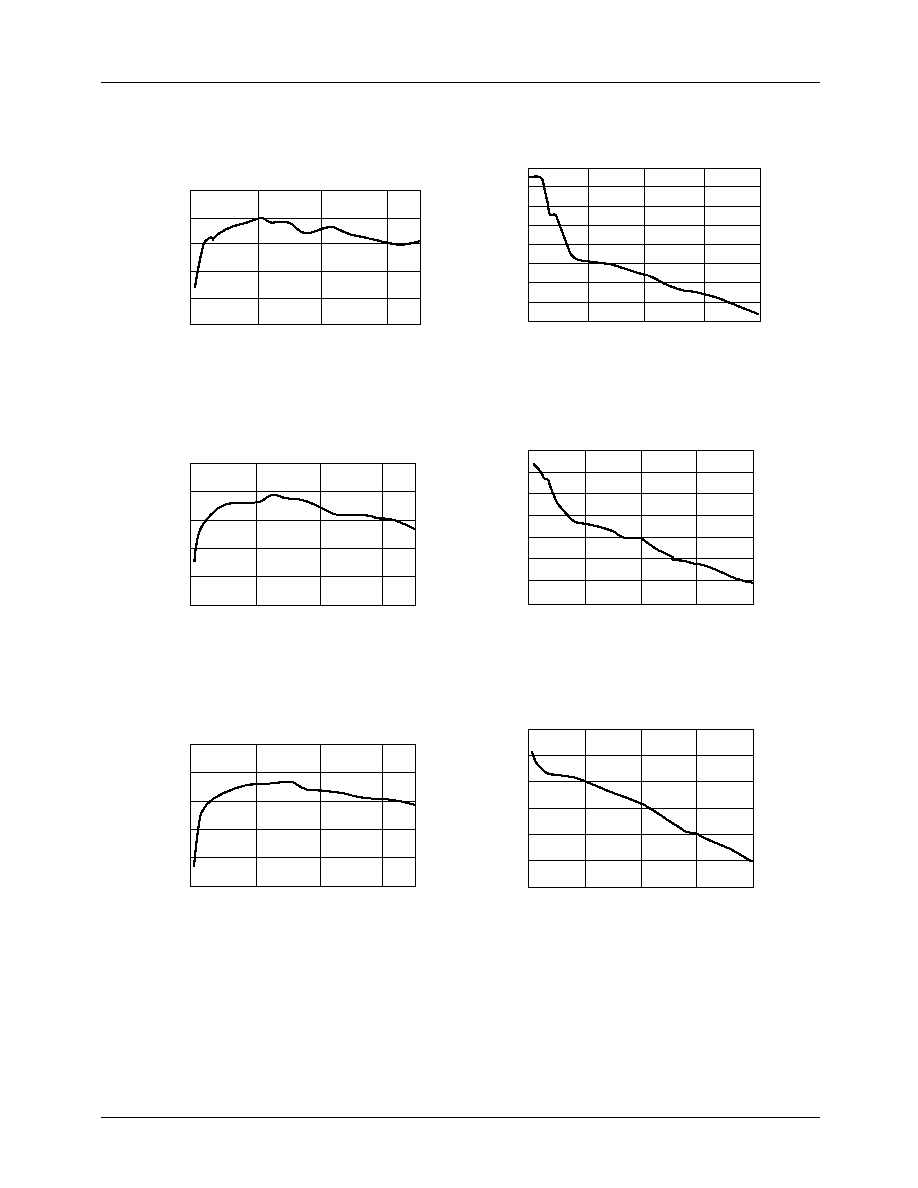
Typical Operating Characteristics
1
Note:
1. Data taken with circuit of Figure 1.
Efficiency vs Output Current (FOSC = 400 KHz)
Efficiency (%)
Output Current (A)
100
90
80
70
60
50
0
2
4
6
Efficiency vs Output Current (FOSC = 650 KHz)
Efficiency (%)
Output Current (A)
100
90
80
70
60
50
0
2
4
6
Efficiency vs Output Current (FOSC = 1 MHz)
Efficiency (%)
Output Current (A)
100
90
80
70
60
50
0
2
4
6
Load Regulation (FOSC = 1 MHz)
V
OUT
Output Current (A)
Output Current (A)
3.36
3.35
3.34
3.33
3.32
3.31
3.3
0
2
4
6
65-5033-03
8
Load Regulation (FOSC = 650 KHz)
V
OUT
3.37
3.36
3.35
3.34
3.33
3.32
3.31
3.3
0
2
4
6
8
Output Current (A)
Load Regulation (FOSC = 400 KHz)
V
OUT
3.38
3.37
3.36
3.35
3.34
3.33
3.32
3.31
3.3
0
2
4
6
8