 | –≠–ª–µ–∫—Ç—Ä–æ–Ω–Ω—ã–π –∫–æ–º–ø–æ–Ω–µ–Ω—Ç: RC5041M | –°–∫–∞—á–∞—Ç—å:  PDF PDF  ZIP ZIP |
Pr
eliminar
y Infor
mation
Electronics
Semiconductor Division
Features
∑ Programmable output from 2.1V to 3.5V using integrated
4-bit DAC
∑ 87% efficiency
∑ Oscillator frequency adjustable from 200KHz to 1MHz
∑ On-chip Power Good function
∑ Excellent transient response
∑ Over-Voltage Protection
∑ Short Circuit Protection
∑ Power Good Function
∑ Precision trimmed low TC voltage reference
∑ 16 pin SOIC package
∑ Meets Intel Pentium VRM specifications using minimum
number of external components
Applications
∑ Programmable power supply for P54C, P55C, K6, and
M2 based CPU motherboards
∑ VRM module for Pentium and equivalent CPU's
∑ Programmable power supply for high current
microprocessors
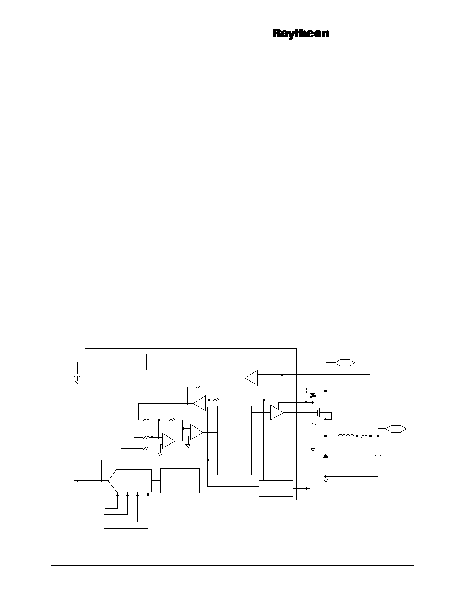
Description
The RC5041 is a non-synchronous DC-DC controller IC
which provides an accurate, programmable output for
Pentium CPU applications. Using an integrated 4-bit DAC to
accept a voltage identification (VID), the RC5041 can gener-
ate precise output voltages between 2.1V and 3.5V in
100mV increments. Output load currents in excess of 10A
can be delivered using minimal external circuitry. The
RC5041 is designed to operate in a standard PWM control
mode under heavy load conditions and in PFM control mode
while supplying light loads for optimal efficiency. An on-
board precision low TC voltage reference eliminates the
requirement for external components in order to achieve
tight voltage regulation. The Pentium CPU is continuously
protected by an integrated Power Good function, which
sends an active-low interrupt signal to the CPU in the event
that the output voltage is out of tolerance. The internal oscil-
lator can be programmed to operate over a range of 200KHz
to 1MHz to allow flexibility in choosing external compo-
nents.
Block Diagram
DIGITAL
CONTROL
≠
+
1.24V
REFERENCE
4-BIT
DAC
65-5041-01
POWER
GOOD
OSCILLATOR
RC5041
PWRGD
VID0
VID1
VID2
VID3
≠
+
≠
+
≠
+
VIN
VO
VREF
+5V
+12V
RC5041
Programmable DC-DC Converter for Pentium
Æ
P55C, K6TM, and 6x86MXTM (M2) Processors
Rev. 0.9.5
PRELIMINARY INFORMATION
describes products that are not in full production at the time of printing. Specifications are based on design goals
and limited characterization. They may change without notice. Contact Raytheon Electronics for current information.
Pentium is a registered trademark of Intel Corporation.
K6 is a trademark of AMD Corporation.
6x86MX is a trademark of Cyrix Corporation.

RC5041
PRODUCT SPECIFICATION
2
Pr
eliminar
y Infor
mation
Pin Assignments
Pin Definitions
Pin Number Pin Name
Pin Function Description
1
CEXT
Oscillator capacitor connection.
Connecting an external capacitor to this pin sets
the internal oscillator frequency from 200 KHz to 1 MHz. Layout of this pin is critical to
system performance. See Application Information for details.
2
PWRGD
Power Good output flag.
Open collector output will be at logic HIGH under normal
operation. Logic LOW indicates output voltage is not within
±
10% of nominal.
3
IFB
High side current feedback.
Pins short 4 and 5 are used as the inputs for the current
feedback control loop and as the short circuit current sense points. Layout of these
traces is critical to system performance. See Application Information for details.
4
VFB
Voltage feedback.
Pin 5 is used as the input for the voltage feedback control loop and
as the low side current feedback input. Layout of this trace is critical to system
performance. See Application Information for details.
5
VCCA
Analog V
CC
.
Connect to system 5V supply and decouple to ground with 0.1
µ
F
ceramic capacitor.
6
VCCD
Digital V
CC
.
Connect to system 5V supply and decouple to ground with 4.7
µ
F
tantalum capacitor.
7
GNDP
Power ground.
Return pin for high currents flowing in pins 8 and 9 (HIDRV and
VCCQP). Connect to low impedance ground. See Application Information for details.
8
HIDRV
FET driver output.
Connect this pin to the gate of the N-channel MOSFETs M1 and
M2 in Figures 1 and 2. The trace from this pin to the MOSFET gates should be kept as
short as possible (less than 0.5"). See Application Information for details.
9
VCCQP
Power V
CC
for FET Driver.
VCCQP must be connected to a voltage of at least
VCCA + V
GS,ON
(M1). See Application Information for details.
10
GNDD
Digital ground.
Return path for digital logic. This pin should be connected to system
ground so that ground loops are avoided. See Application Information for details.
11
GNDA
Analog ground.
Return path for low power analog circuitry. Connect to system ground
so that ground loops are avoided. See Application Information for details.
12
VREF
Reference voltage test point.
This pin provides access to the DAC output and
should be decoupled to ground using a 0.1
µ
F capacitor. No load should be connected
to this pin.
13≠16
VID3≠
VID0
Voltage identification (VID) code inputs.
These open collector/TTL compatible
inputs will program the output voltage over the ranges specified in Table 1.
CEXT
PWRGD
IFB
VFB
VCCA
VCCD
GNDP
HIDRV
16
65-5041-02
15
14
13
12
11
10
9
VID0
VID1
VID2
VID3
VREF
GNDA
GNDD
VCCQP
1
2
3
4
5
6
7
8
PRODUCT SPECIFICATION
RC5041
3
Pr
eliminar
y Infor
mation
Absolute Maximum Ratings
1
Notes:
1. Functional operation under any of these conditions is not implied. Permanent damage may occur if the device is subjected to
conditions outside these ratings.
Operating Conditions
Control Supply Voltages, VCCA and VCCD
7V
FET Supply Voltage, VCCQP
13V
Voltage Identification Code Inputs, VID3-VID0
7V
Junction Temperature, T
J
150∞C
Storage Temperature, T
S
-65 to 150∞C
Lead Soldering Temperature, 10 seconds
300∞C
Parameter
Min.
Typ.
Max.
Units
Control Supply Voltages, VCCA and VCCD
4.75
5
5.25
V
Driver Supply Voltage, VCCQP
9
10
12
V
VID Code Input Voltage, Logic HIGH
2
V
VID Code Input Voltage, Logic LOW
0.8
V
PWRGD HIGH Threshold
±
7
%VREF
PWRGD LOW Threshold
±
10
%VREF
Ambient Temperature, T
A
0
70
∞
C
Electrical Specifications
(V
CCA
= 5V, V
OUT
= 2.8V, f
osc
= 300 KHz, and T
A
= +25
∞
C using circuit in Figure 1, unless otherwise noted)
The
∑
denotes specifications which apply over the full operating temperature range.
Parameter
Conditions
Min.
Typ.
Max.
Units
Output Voltage
See Table 1
∑
3.5
V
Output Current
13
A
Initial Voltage Setpoint
I
LOAD
= 0.8A
±
20
mV
Output Temperature Drift
T
A
= 0 to 60
∞
C
∑
+10
mV
Load Regulation
I
LOAD
= 0.8A to 10A
∑
-20
mV
Line Regulation
V
IN
= 4.75V to 5.25V
∑
±
2
mV
Output Ripple/Noise, pk-pk
20MHz BW, I
LOAD
= 10A
20
mV
Data Bits
V
CC
P
VID3
VID2
VID1
VID0
(VDC)
1
1
1
1
No CPU
1
1
1
0
2.1
1
1
0
1
2.2
1
1
0
0
2.3
1
0
1
1
2.4
1
0
1
0
2.5
1
0
0
1
2.6
1
0
0
0
2.7
0
1
1
1
2.8
0
1
1
0
2.9
0
1
0
1
3.0
0
1
0
0
3.1
0
0
1
1
3.2
0
0
1
0
3.3
0
0
0
1
3.4
0
0
0
0
3.5
Data Bits
V
CC
P
VID3
VID2
VID1
VID0
(VDC)
Table 1. Voltage Identification Codes for P55/K6

RC5041
PRODUCT SPECIFICATION
4
Pr
eliminar
y Infor
mation
Notes:
1. Steady State Voltage Regulation includes Initial Voltage Setpoint, DC load regulation, outut ripple/noise and temperature drift.
2. These specifications assume a minimum of 20, 1
µ
F ceramic capacitors are placed directly next to the CPU in order to provide
adequate high-speed decoupling. For motherboard applications, the PCB layout must exhibit no more than 0.5m
parasitic
resistance and 1nH parasitic inductance between the converter output and the CPU.
Test Circuits
Figure 1. Standard Test or Application Schematic
Output Voltage Regulation
Steady State
1
Transient
2
V
OUT
= 2.8V, I
LOAD
= 0 to 10A
I
LOAD
= 0.8 to 9.5A, 30A/
µ
S
∑
∑
2.74
2.70
2.80
2.80
2.90
2.90
V
V
Efficiency
I
LOAD
= 10A, V
OUT
= 2.8V
∑
80
85
%
Output Driver Rise and Fall Time
See Figure 2
50
ns
Turn-on Response Time
I
LOAD
= 0A to 10A
10
ms
Oscillator Range
80
300
1000
KHz
Oscillator Frequency
C
EXT
= 100 pF
300
KHz
Maximum Duty Cycle
90
95
%
Electrical Specifications
(continued)
(V
CCA
= 5V, V
OUT
= 2.8V, f
osc
= 300 KHz, and T
A
= +25
∞
C using circuit in Figure 1, unless otherwise noted)
The
∑
denotes specifications which apply over the full operating temperature range.
Parameter
Conditions
Min.
Typ.
Max.
Units
VO
GND
VID2
VID3
VID1
VID0
VCC
PWRGD
U1
RC5041
VCC
VCC
C11
0.1
µ
F
R6
10K
R4
10K
65-5041-03
10K
10K
R3
R2
10K
R1
CEXT
100pF
C7
0.1
µ
F
C6
1.0
µ
F
DS1
CIN
COUT
DS2
C12
+12V
1
µ
F
L1
1.0
µ
H
M1
C8
0.1
µ
F
RSENSE
6m
8
7
6
5
4
3
2
1
9
10
11
12
13
14
15
16
VREF
L2
2.5
µ
H
C4
0.1
µ
F
PRODUCT SPECIFICATION
RC5041
5
Pr
eliminar
y Infor
mation
Table 2. Bill of Materials for a 4-Bit Non-Synchronous DC-DC Converter
Note:
1. The inductor L2 is recommended to isolate the 5V ipower supply from current surges caused by the MOSFET switching. This
inductor is not required for the proper operation of the DC-DC converter and can be substituted with a ferrite beads inductor
or omitter completely.
Table 3. Part Selection Table
Item
Description
Comments
C4
Ceramic Capacitor, 0.1
µ
F, X7R, SMT0805
C12
Ceramic Capacitor, 1
µ
F, X7R, SMT0805
C8
Ceramic Capacitor, 0.1
µ
F, X7R, SMT0805
C
EXT
Ceramic Capacitor, 100pF, X7R, SMT0805
C6
Ceramic Capacitor, 1
µ
F, X7R, SMT0805
C11
Ceramic Capacitor, 0.1
µ
F, X7R, SMT0805
C7
Capacitor, 0.1
µ
F, X7R, SMT0805
C
IN
Capacitor, Al-Elect, 1200
µ
F, 10v, 10 x 20 radial
See Table 3
C
OUT
Capacitor, Al-Elect, 1500
µ
F, 6.3v, 10 x 20 radial
See Table 3
DS1
Schottky Diode, MBR2535CT
DS2
Schottky Diode, 1N5817
L1
Output Inductor, 1.0
µ
H, Toroid, 6 turns 17AWG
L2
Input Inductor, 2.5
µ
H, Toroid, 10 turns 17AWG
See Note 1
R
SENSE
Sense Resistor, CuNi Allow Wire, 1W, 6m
, 10%
R1
10
Resistor, 1/8W, 5%, SMT0805
R2
10
Resistor, 1/8W, 5%, SMT0805
R3
10
Resistor, 1/8W, 5%, SMT0805
R4
10
Resistor, 1/8W, 5%, SMT0805
R6
10
Resistor, 1/8W, 5%, SMT0805
M1
N-ch Power FET
See Table 2
U1
PWM Controller, Raytheon RC5041M
K6 CPU
Output Voltage
I
MAX
Raytheon
DC-DC Converter
CIN
Sanyo
10MV1200GX
COUT
Sanyo
6MV1500GX
MOSFET
166 MHz
2.9V
6.25A
RC5041
1x
2x
IRL3103
200 MHz
2.9V
7.5A
1x
2x
IRL3103
233 MHz
3.2V
9.5A
2x
4x
IRL3103
266 MHz
3.2V
13.0A
3x
6x
IRL2203
300 MHz+
2.1V
5.6A
1x
2x
IRL3103