 | –≠–ª–µ–∫—Ç—Ä–æ–Ω–Ω—ã–π –∫–æ–º–ø–æ–Ω–µ–Ω—Ç: RMLA31400 | –°–∫–∞—á–∞—Ç—å:  PDF PDF  ZIP ZIP |
Raytheon RF Components
362 Lowell Street
Andover, MA 01810
Released October 31, 2002
Page 1
www.raytheonrf.com
Characteristic performance data and specifications are subject to change without notice.
ADVANCED INFORMATION
Raytheon
RF Components
RMLA31400
31-40 GHz Low Noise Amplifier MMIC
Description
!
1.8 dB Typical Noise Figure
!
20 dB Small Signal Gain
!
Single +1.9 Volt Supply
!
16 mA Supply Current
!
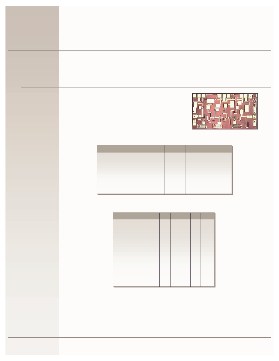
Chip size 2.25 mm x 1.25 mm x 100
µ
m
Features
The RMLA31400 is a 3-stage GaAs Low Noise MMIC Amplifier designed for operation from 31 to 40
GHz. The amplifier operates on a single positive supply voltage and is
ideal for low noise
applications in point to point radios, point to multi-point communications, LMDS, and other millimeter
wave applications. The RMLA31400 is fabricated on Raytheon's production Metamorphic High
Electron Mobility Transistor (MHEMT) process and is sufficiently versatile to serve in a variety of low
noise amplifier applications.
Electrical
Characteristics
(At 25∞C),
50
system,
Vd=+1.9 V,
Supply Current
Id=16 mA
Absolute
Ratings
Parameter
Min
Typ
Max
Unit
Frequency Range
31
40
GHz
Noise Figure
1.8
dB
Gain Small Signal
20
dB
Gain Flatness
+/- 1
dB
P1dB
-2
dBm
Power Out Saturated
0
dBm
Supply Current
16
mA
Input Return Loss
10
dB
Output Return Loss
>10
dB
Parameter
Symbol
Value
Unit
Positive DC Voltage (+1.9V Typical)
Vd
+ 2.5
Volts
Positive DC Current
I
D
117
mA
RF Input Power (from 50
source)
P
IN
0
dBm
Operating Base plate Temperature
T
C
-30 to +85
∞C
Storage Temperature Range
T
stg
-55 to +125
∞C
Thermal Resistance
R
jc
441
∞C/W
(Channel to Backside)
Raytheon RF Components
362 Lowell Street
Andover, MA 01810
Released October 31, 2002
Page 2
www.raytheonrf.com
Characteristic performance data and specifications are subject to change without notice.
ADVANCED INFORMATION
Raytheon
RF Components
RMLA31400
31-40 GHz Low Noise Amplifier MMIC
CAUTION: THIS IS AN ESD SENSITIVE DEVICE.
Chip carrier material should be selected to have GaAs compatible thermal coefficient of expansion
and high thermal conductivity such as copper molybdenum or copper tungsten. The chip carrier
should be machined, finished flat, plated with gold over nickel and should be capable of withstanding
325∞C for 15 minutes.
Die attachment for power devices should utilize Gold/Tin (80/20) eutectic alloy solder and should
avoid hydrogen environment for MHEMT devices. Note that the backside of the chip is gold plated and
is used as RF and DC Ground.
These GaAs devices should be handled with care and stored in dry nitrogen environment to prevent
contamination of bonding surfaces. These are ESD sensitive devices and should be handled with
appropriate precaution including the use of wrist-grounding straps. All die attach and wire/ribbon bond
equipment must be well grounded to prevent static discharges through the device.
Recommended wire bonding uses 3 mil wide and 0.5 mil thick gold ribbon with lengths as short as
practical allowing for appropriate stress relief. The RF input and output bonds should be typically
0.012" long corresponding to a typical 2 mil gap between the chip and the substrate material.
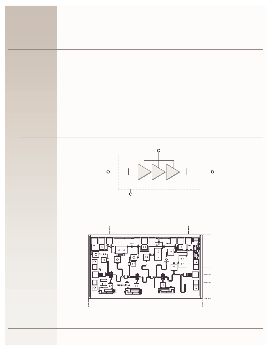
Application
Information
Functional
Block Diagram
RF IN
RF OUT
Drain
Supply Vd
Ground
(Back of Chip)
MMIC Chip
Chip Layout and
Bond Pad
Locations
(Chip Size=2.254 mm
x 1.254 mm x 100
µ
m.
Back of Chip is RF and
DC Ground)
Dimensions in mm
0.317
0.617
0.467
0.0
0.0
2.254
1.254
0.418
1.261
1.979
Raytheon RF Components
362 Lowell Street
Andover, MA 01810
Released October 31, 2002
Page 3
www.raytheonrf.com
Characteristic performance data and specifications are subject to change without notice.
ADVANCED INFORMATION
Raytheon
RF Components
RMLA31400
31-40 GHz Low Noise Amplifier MMIC
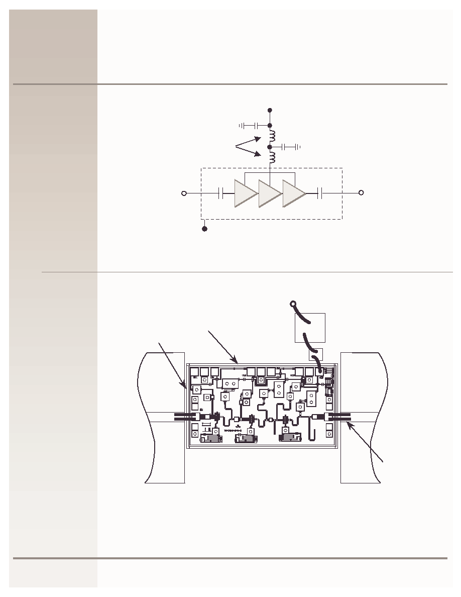
Recommended
Application
Schematic
Circuit Diagram
RF IN
RF OUT
Drain Supply
(Vd=+1.9V)
Ground
(Back of Chip)
MMIC Chip
100pF
10000pF
L
L
Bond Wire Ls
Vd
(Positive)
100pF
10000pF
RF
Input
RF
Output
Alumina
50-Ohm
Alumina
50-Ohm
2 mil Gap
L< 0.015"
(4 Places)
Die-Attach
80Au/20Sn
Note:
Use 0.003" x 0.0005" Gold Ribbon for bonding. RF input and output bonds should be less than 0.015" long with stress relief.
Vd should biased from 1 positive supply. Vg should be biased from 1 negative supply.
Recommended
Assembly
Diagram

Raytheon RF Components
362 Lowell Street
Andover, MA 01810
Released October 31, 2002
Page 4
www.raytheonrf.com
Characteristic performance data and specifications are subject to change without notice.
ADVANCED INFORMATION
Raytheon
RF Components
RMLA31400
31-40 GHz Low Noise Amplifier MMIC
Step 1: Turn off RF input power.
Step 2: Connect the DC supply ground to the
ground of the chip carrier.
Step 3: Slowly apply positive drain bias supply
voltage of +1.9 V to Vd.
Step 4: Observe drain current (Id)~ 16 mA.
Step 4: After the bias condition is established, the
RF input signal may now be applied at the
appropriate frequency band.
Step 5: Follow turn-off sequence of:
(i) Turn off RF input power.
(ii) Turn down and off drain voltage (Vd).
CAUTION: The following sequence of steps must be followed to properly test the amplifier.
Recommended
Procedure
for Biasing and
Operation
RMLA31400 Noise Figure Vs. Frequency
Vd=1.9V, Id=16mA, T=25∞C
0
1
2
3
4
5
6
28
29
30
31
32
33
34
35
36
37
38
39
40
Frequency (GHz)
N
o
i
s
e
F
i
gur
e
(
dB
)
Performance
Data

Raytheon RF Components
362 Lowell Street
Andover, MA 01810
Released October 31, 2002
Page 5
www.raytheonrf.com
Characteristic performance data and specifications are subject to change without notice.
ADVANCED INFORMATION
Raytheon
RF Components
RMLA31400
31-40 GHz Low Noise Amplifier MMIC
Performance
Data
RMLA31400 S-Parameters Vs. Frequency
Vd=1.9V, Id=16mA Temperature= 25
o
C
-50
-45
-40
-35
-30
-25
-20
-15
-10
-5
0
5
10
15
20
25
30
20
25
30
35
40
45
50
Frequency (GHz)
Si
j
(
d
B
)
S11
S21
S22
S12
RMLA31400 Pow er @1dB Compression Vs. Frequency
Vd=1.9V, Id=16mA Temperature= 25
o
C
-5
0
5
10
30
31
32
33
34
35
36
37
38
39
40
41
Frequency (GHz)
P1
d
B
(
d
B
m
)