Raytheon RF Components
362 Lowell Street
Andover, MA 01810
Revised January 25, 2002
Page 1
Characteristic performance data and specifications are subject to change without notice.
PRODUCT INFORMATION
www.raytheonrf.com
The Raytheon RMM2080 GaAs MMIC device is a three-stage distributed medium-power amplifier with gain control
capability. The circuit incorporates ion-implanted, 0.5-
µ
m gate MESFET devices fabricated on a semi-insulating
GaAs substrate. The first two stages are 4-cell distributed amplifiers utilizing dual-gate FETs for improved gain per
stage and to facilitate gain control (4x125µm & 4x250µm). The third stage is a 3-cell distributed dual-gate FET
amplifier designed for high output power and efficiency (3x500µm). The RMM2080 amplifier is designed for
interconnection with microstrip transmission media using fully automatic assembly techniques.
2-18 GHz Bandwidth
24 dB Typical Gain
±2 dB Gain Flatness
20 dBm Output Power Typical
Three Stages of Distributed Amplification
Gain Control of up to 70 dB range
Dual-Gate Ion-Implanted 0.5
µ
m FETs
Chip Size: 4.14mm x 3.22mm x 0.1mm
Features
Absolute
Maximum
Ratings
Description
Notes:
1. Typical range of the negative gate voltage is -0.9 to 0.0V to set typical Idq of 300 mA.
2. GC1 and GC2 of +1.5V and VG23=open corresponds to maximum gain and power.
RMM2080
2-18 GHz Wideband Variable-Gain
Driver Amplifier
Electrical
Characteristics
(At 25∞C)
50
system,
Vd=+7 V,
Quiescent current (Idq)
=300 mA
GC1, GC2= +1.5 V
Parameter
Min
Typ
Max
Unit
Frequency Range
2
-
18
GHz
Gate Supply Voltage (Vg)
1
-0.7
Volts
RF Output Power @ -1 dBc
20
dBm
Small Signal Gain
18
24
dB
Gain Flatness vs. Freq.
± 2
dB
Input/Output Return Loss
7
dB
Parameter
Min
Typ
Max
Unit
Gain Control Range
70
dB
Gain Control Voltage,
-5
+1.5
Volts
GC1&2
2
Parameter
Symbol
Value
Unit
Positive Drain DC Voltage (+7V typ)
Vd
+8
V
Negative DC Voltage
Vg
-2
V
Simultaneous (Vd-Vg)
Vgd
10
V
Positive DC Current
Id
400
mA
RF Input Power (from 50
source)
P
IN
(CW)
+8
dBm
Operating Baseplate Temperature
T
case
-30 to 85
∞C
Storage Temperature Range
T
storage
-55 to 125
∞C
Thermal Resistance
R
jc
22
∞C/W
(channel to backside)

Raytheon RF Components
362 Lowell Street
Andover, MA 01810
Revised January 25, 2002
Page 2
Characteristic performance data and specifications are subject to change without notice.
PRODUCT INFORMATION
www.raytheonrf.com
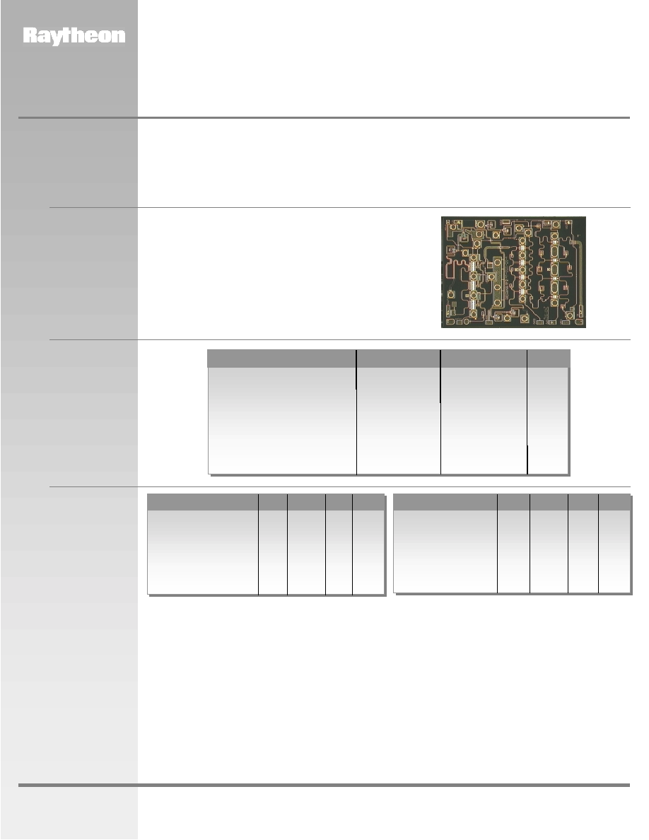
Figure 1
Block Diagram and
Circuit Schematic
Figure 2
Location and Size of
Bonding Pads
Dimensions in inches
RMM2080
2-18 GHz Wideband Variable-Gain
Driver Amplifier

Raytheon RF Components
362 Lowell Street
Andover, MA 01810
Revised January 25, 2002
Page 3
Characteristic performance data and specifications are subject to change without notice.
PRODUCT INFORMATION
www.raytheonrf.com
VD
VG
Figure 3
Example of
Assembled Module
GC
RMM2080
2-18 GHz Wideband Variable-Gain
Driver Amplifier

Raytheon RF Components
362 Lowell Street
Andover, MA 01810
Revised January 25, 2002
Page 4
Characteristic performance data and specifications are subject to change without notice.
PRODUCT INFORMATION
www.raytheonrf.com
Performance
Data
-5
0
5
10
15
20
25
30
0.00
5.00
10.00
15.00
20.00
25.00
30.00
35.00
1.5
1
0.5
0
-0.5
-1
-1.5
-2
Vcontrol (V)
2GHz
10GHz
18GHz
P1
Gain
10
12
14
16
18
20
22
24
26
28
30
0
2
4
6
8
10 12 14 16 18 20
Frequency (GHz)
35
30
25
20
15
10
5
0
0
2
4
6
8
10 12 14 16 18 20
Frequency (GHz)
S22
S11
The above data is derived from fixtured measurements which include 3 parallel, 1 mil diameter, 15 mil long, gold bond wires
connected to the RF input and output.
The Id @ 1 dB compression increases to approximately 0.45 A. The dc supply should be able to support the required current to
achieve the above performance.
RMM2080
2-18 GHz Wideband Variable-Gain
Driver Amplifier
Input & Output Return Loss
Vd=7.0V, Id=0.3A, GC1,2=1.5V
Small Signal Gain
Vd=7.0V, Id=0.3A, GC1,2=1.5V
Gain & Pout vs, Control Voltage
Vd=7.0V, Id=0.3A @ GC1,2=1.5V