 | –≠–ª–µ–∫—Ç—Ä–æ–Ω–Ω—ã–π –∫–æ–º–ø–æ–Ω–µ–Ω—Ç: R1100 | –°–∫–∞—á–∞—Ç—å:  PDF PDF  ZIP ZIP |
Document Outline
- ˛ˇ
- ˛ˇ
- ˛ˇ
- ˛ˇ
- ˛ˇ
- ˛ˇ
- ˛ˇ
- ˛ˇ
- ˛ˇ
- ˛ˇ
- ˛ˇ
- ˛ˇ
- ˛ˇ
- ˛ˇ
- ˛ˇ
- ˛ˇ
- ˛ˇ
- ˛ˇ
- ˛ˇ
- ˛ˇ
- ˛ˇ
- ˛ˇ
- ˛ˇ
- ˛ˇ
- ˛ˇ
- ˛ˇ

RDC
RDC
RDC
RDC
Æ
RISC DSP Controller
R1100
RDC Semiconductor Co.
Rev 1.2
Subject to change without notice
1
R1100
16-Bit RISC Microcontroller User's Manual
RDC
RDC
RDC
RDC
RISC DSP Controller
RDC Semiconductor Co., Ltd
http:\\www.rdc.com.tw
Tel. 886-3-666-2866
Fax 886-3-563-1498

RDC
RDC
RDC
RDC
Æ
RISC DSP Controller
R1100
RDC Semiconductor Co.
Rev 1.2
Subject to change without notice
2
Contents
------------------------------------------------------------------------------------ page
1. Features ---------------------------------------------------------------------------4
2. Block Diagram ------------------------------------------------------------------5
3. Pin Configuration --------------------------------------------------------------6
4. Pin Description ---------------------------------------------------------------- 9
5. Basic Application System Block ------------------------------------------- 15
6. Oscillator Characteristics --------------------------------------------------- 16
7. Read/Write timing Diagram ----------------------------------------------- 15
8. Execution Unit ---------------------------------------------------------------- 20
8.1
General Register
---------------------------------------------------------- 20
8.2
Segment Register
--------------------------------------------------------- 20
8.3
Instruction Pointer and Status Flags Register
-------------------------- 21
8.4
Address Generation
-------------------------------------------------------- 22
9. Peripheral Control Block Register ----------------------------------------- 23
10. System Clock ------------------------------------------------------------------ 25
11. Reset ----------------------------------------------------------------------------- 28
12. Bus Interface Unit ------------------------------------------------------------ 30
12.1
Memory and I/O Interface
---------------------------------------------- 30
12.2
Data Bus
------------------------------------------------------------------ 30
12.3
Wait States
--------------------------------------------------------------- 31
12.4
Bus Hold
------------------------------------------------------------------ 32
13. Chip Select Unit--------------------------------------------------------------- 34
13.1
UCS
---------------------------------------------------------------------- 34
13.2
LCS
----------------------------------------------------------------------- 35
13.3
MCSx
-------------------------------------------------------------------- 36
13.4
PCSx
--------------------------------------------------------------------- 38
14. Interrupt Controller Unit ------------------------------------------------- 40
14.1
Master Mode and Slave Mode
----------------------------------------- 40
14.2
Interrupt Vector, Type and Priority
---------------------------------- 41
14.3
Interrupt Request
------------------------------------------------------- 42
14.4
Interrupt Acknowledge
------------------------------------------------ 42
14.5
Programming Register
------------------------------------------------- 42
15. DMA Unit ---------------------------------------------------------------------- 56

RDC
RDC
RDC
RDC
Æ
RISC DSP Controller
R1100
RDC Semiconductor Co.
Rev 1.2
Subject to change without notice
3
15.1
DMA Operation
--------------------------------------------------------- 56
15.2
External Requests
-------------------------------------------------------- 61
16. Timer Control Unit----------------------------------------------------------- 63
16.1
Timer/Counter Unit Output Mode
------------------------------------ 70
17. Asynchronous Serial Port--------------------------------------------------- 71
18. Synchronous Serial Port ---------------------------------------------------- 75
19. PIO Unit ---------------------------------------------------------------------- 79
19.1
PIO Multi-Function Pin list Table
----------------------------------- 79
20. Instruction Set Opcodes and Clock Cycle------------------------------- 82
20.1
R1100 Execution Timings
-------------------------------------------- 86
21. I/O Characteristica of each pin ------------------------------------------- 87
22. Add DC/AC Characteristics -----------------------------------------------90
23. Package Information--------------------------------------------------------100
24. Revision History ------------------------------------------------------------102
Appendix A -------------------------------------------------------------------103

RDC
RDC
RDC
RDC
Æ
RISC DSP Controller
R1100
RDC Semiconductor Co.
Rev 1.2
Subject to change without notice
4
High Speed 16-Bit Microcontroller
1. Features
Five-stages pipeline
RISC architecture
Integrated PLL(*1~*8)
Maximum frequency is 80 MHz; External bus, Internal bus and core are in the same clock base
Bus interface
- Multiplexed address and Data bus
- Supports direct address bus [A19 : A0]
- 8-bit or 16-bit external bus dynamic access
- 1M byte memory address space
- 64K byte I/O space
Software is compatible with generic 80C186 microprocessor
Support two Asynchronous serial channels with hardware handshaking signals.
External bus, Internal bus and core are in the same clock base
Supports 32 PIO pins
Three independent 16-bit timers and one independent programmable watchdog timer
The Interrupt controller with seven maskable external interrupts and one non-maskable external interrupt(NMI)
Two independent DMA channels
Programmable chip-select logic for Memory or I/O bus cycle decoder
Programmable wait-state generator
The I/O pin output is 3.3 volt level and the input is 3.3 volt to 5 volt tolerance.
3.3V operation voltage
Support CPU ID
RDC
RDC
RDC
RDC
Æ
RISC DSP Controller
R1100
RDC Semiconductor Co.
Rev 1.1
Subject to change without notice
5
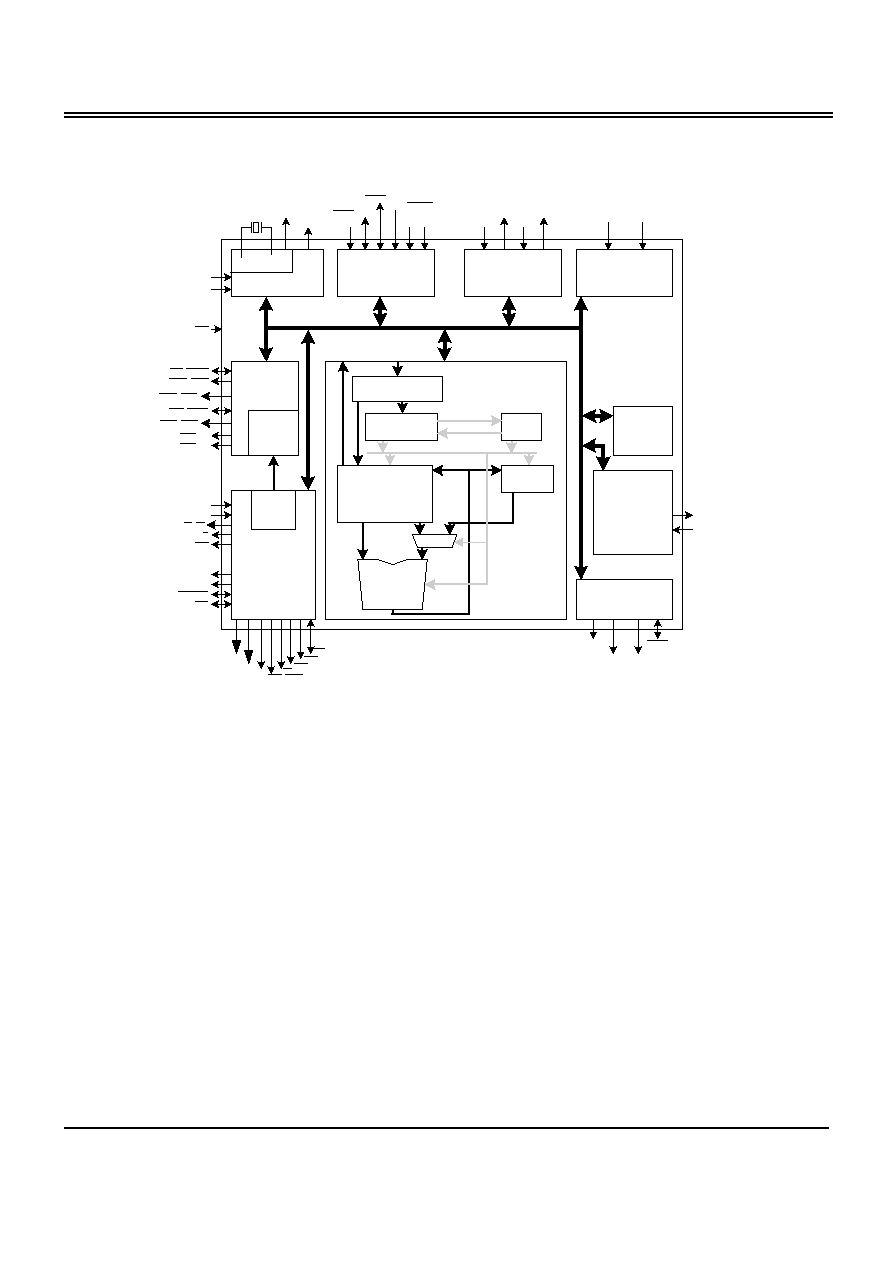
2.Block Diagram
DMA
Unit
PSRAM
Control
Unit
Chip
Select
Unit
Refresh
Control
Unit
Bus
Interface
Unit
PIO
Unit
Synchronous
Serial Interface
Timer Control
Unit
Interrupt
Control Unit
Clock & Power
Management
Asynchro-
nous Serial
Port
Instruction
Queue (64bits)
Instruction
Decoder
Register
File
General,
Segment,
Eflag Register
ALU
(Special,
Logic,
Adder,
BSF)
Micro
ROM
EA / LA
Address
Control Signal
Execution
Unit
X1
X2
CLKOUTA
CLKOUTB
INT4
INT0
TMRIN0
TMROUT0
TMRIN1
TMROUT1
DRQ0
DRQ1
TXD
RXD
SCLK
SDEN0 SDEN1
SDATA
A19~A0
AD15~AD0
ALE
BHE/ADEN
WR
WLB
WHB
RD
VCC
GND
LCS/ONCE0
MCS3/RFSH
UCS/ONCE1
PCS5/A1
PCS6/A2
ARDY
SRDY
S2~S0
DT/R
DEN
HOLD
HLDA
S6/CLKDIV2
UZI
INT3/INTA1/IRQ
INT2/INTA0
INT1/SELECT
NMI
RST
MCS2-MCS0
PCS3-PCS0
PLL