PO 34
www.recom-international.com
POWERLINE - DC/DC-Converter
A-Series, 8 Watt, DIP24, Regulated & Wide Input Range (Dual Output)
8 Watts in DIP24 Package
Include 3.3VDC Output
Efficiency up to 86%
Regulated Outputs
Low Profile, 10.2 mm Height
No Derating to 71∞C
No other Components required
Five-Sided EMI Shield
Over Current Protection,
Continuous
MTBF 7.189 x 10
5
Hours
2 Year Warranty
Standard and SMT-Pinning
UL 1950 Component Recognised
Features
Part Number
Input
Output
Output
Efficiency
Range
Voltage
Current
(%)
RP08-1233SA
9-18 VDC
3.3 VDC
2000 mA
81
RP08-1205SA
9-18 VDC
5 VDC
1500 mA
82
RP08-1212SA
9-18 VDC
12 VDC
666 mA
86
RP08-1215SA
9-18 VDC
15 VDC
533 mA
83
RP08-1205DA
9-18 VDC
±5 VDC
±800 mA
83
RP08-1212DA
9-18 VDC
±12 VDC
±333 mA
84
RP08-1215DA
9-18 VDC
±15 VDC
±267 mA
84
RP08-2433SA
18-36 VDC
3.3 VDC
2000 mA
80
RP08-2405SA
18-36 VDC
5 VDC
1500 mA
84
RP08-2412SA
18-36 VDC
12 VDC
666 mA
83
RP08-2415SA
18-36 VDC
15 VDC
533 mA
83
RP08-2405DA
18-36 VDC
±5 VDC
±800 mA
83
RP08-2412DA
18-36 VDC
±12 VDC
±333 mA
85
RP08-2415DA
18-36 VDC
±15 VDC
±267 mA
85
RP08-4833SA
36-75 VDC
3.3 VDC
2000 mA
80
RP08-4805SA
36-75 VDC
5 VDC
1500 mA
83
RP08-4812SA
36-75 VDC
12 VDC
666 mA
84
RP08-4815SA
36-75 VDC
15 VDC
533 mA
84
RP08-4805DA
36-75 VDC
±5 VDC
±800 mA
84
RP08-4812DA
36-75 VDC
±12 VDC
±333 mA
85
RP08-4815DA
36-75 VDC
±15 VDC
±267 mA
85
Selection Guide
12V, 24V and 48V Input Types
Maximum Capacitive Load
RP08-xx33SA
3300µF
RP08-xx05SA
1600µF
RP08-xx12SA
350µF
RP08-xx15SA
240µF
RP08-xx05DA
±1000µF
RP08-xx12DA
±160µF
RP08-xx15DA
±100µF
August 2002
PO 35
www.recom-international.com
August 2002
POWERLINE - DC/DC-Converter
A-Series, 8 Watt, DIP24, Regulated & Wide Input Range (Dual Output)
Input Voltage Range
12V types nominal
9-18V
24V types nominal
18-36V
48V types nominal
36-75V
Input Filter
Pi Type
Voltage Accuracy
±2%
Voltage Balance, Dual Outputs
±2%
Ripple and Noise, 20MHz BW
50mVp-p
Line Regulation
Single Output ±0.2% max.
Dual Output ±0.2% max.
Load Regulation, FL-1/4FL
Single Output ±2% max.
Dual Output ±1% max.
Temperature Coefficient
±0.02%/∞C
Over Current Protection
Continuous
Control Voltage Referenced to Negative(-)Input Compatability
CMOS, TTL
ON-Control
4.8V min, or Open
OFF-Control
0.4V max. or Short
Switching Frequency
300kHz, typ.
Isolation Voltage
1600VDC
Isolation Resistance
10
9
Isolation Capacitance
300pF max.
Operating Temperature Range
-25∞C to +71∞C
Storage Temperature Range
-55∞C to +125∞C
Cooling
Free-air Convection
EMI/RFI
Five-sided Shield
Case Material
Nickel-Coated Copper with Non-Conductive Base
Dimensions
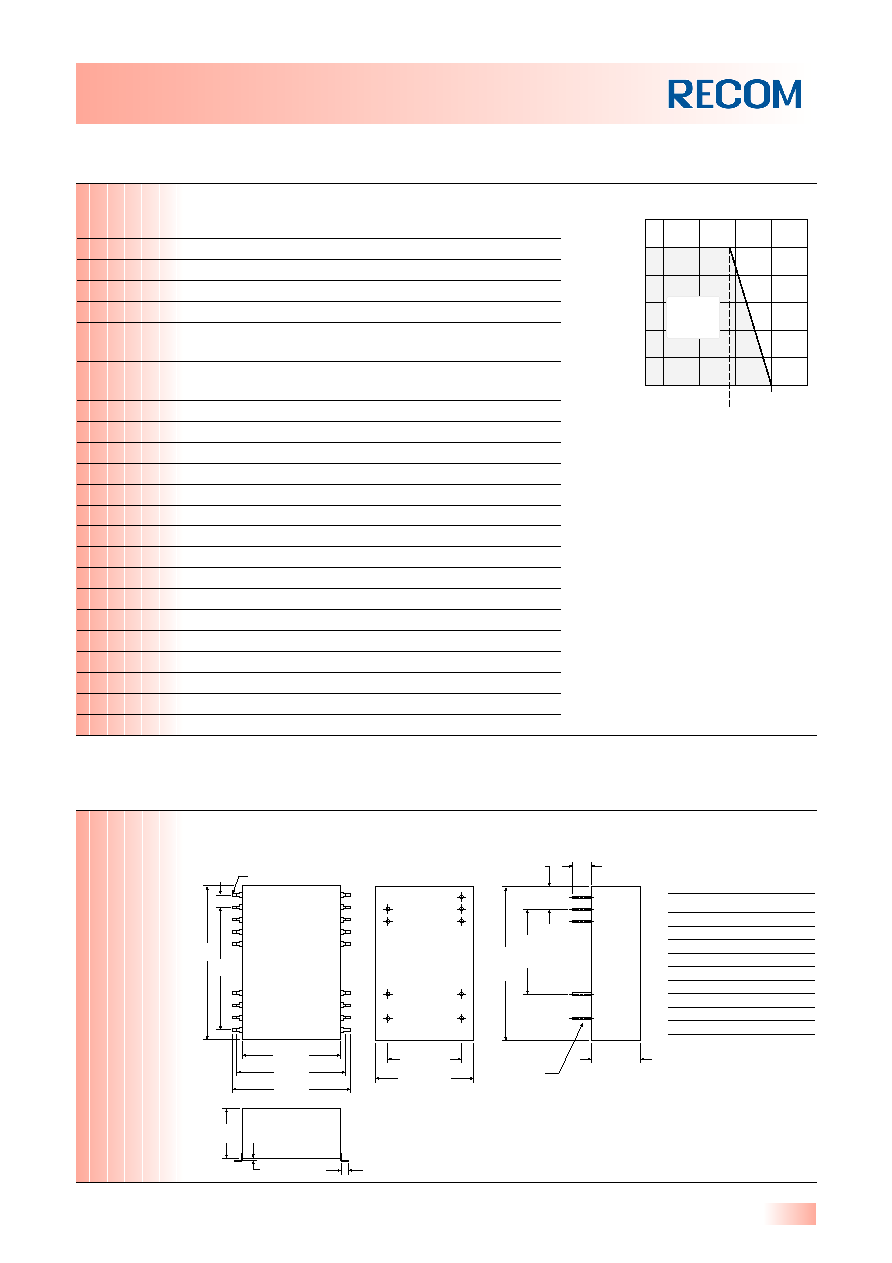
31.8 x 20.3 x 10.2 mm
MTBF (MIL-HDBK-217F TA = 25∞C full load)
7.189 x 10
5
Hours
Specifications
(typical at nominal input and 25∞C unless otherwise noted)
31.80
17.80
4.6
3.8
10.20
0.25 x 0.50
Rectangular Pin
15.20
Bottom
View
20.30
1
2
3
23
22
16
14
9
11
Pin Connections
Pin #
Single
Dual
1
ON/OFF
ON/OFF
2
-Vin
-Vin
3
-Vin
-Vin
9
NC
Com
11
NC
-Vout
14
+Vout
+Vout
16
-Vout
Com
22
+Vin
+Vin
23
+Vin
+Vin
NC = No Connection
Pin Pitch Tolerance ±0.35 mm
Package Style and Pinning (mm)
Output Power (%)
120
80
100
50
-25
125
Ambient Temperature ∞C
0
25
100
60
40
20
Natural
Convection
Cooling
71
75
24
23
22
21
20
16
15
14
13
Bottom View
1
2
3
4
5
9
10
11
12
31.80
2.54
20.32
23.40
25.54
25.40
Pin area 0.1 x 0.25
1.52
0.25
10.90
SMD Package Style
Same spec. as the original DIP spec. and
pin definition, excl. of the SMD type pin.
DIP24 Package Style