7534 Group
SINGLE-CHIP 8-BIT CMOS MICROCOMPUTER
REJ03B0099-0200Z
Rev.2.00
Jun 21, 2004
Rev.2.00 Jun 21, 2004 page 1 of 54
REJ03B0099-0200Z
DESCRIPTION
The 7534 Group is the 8-bit microcomputer based on the 740 family
core technology.
The 7534 Group has a USB, 8-bit timers, and an A/D converter, and
is useful for an input device for personal computer peripherals.
FEATURES
∑
Basic machine-language instructions ....................................... 69
∑
The minimum instruction execution time .......................... 0.34 µs
(at 6 MHz oscillation frequency for the shortest instruction)
∑
Memory size
ROM ............................................... 8K to 16K bytes
RAM .............................................. 256 to 384 bytes
∑
Programmable I/O ports ...................................... 28 (36-pin type)
............................................................................ 24 (32-pin type)
............................................................................ 33 (42-pin type)
∑
Interrupts .................................................... 14 sources, 8 vectors
∑
Timers ............................................................................ 8-bit
3
∑
Serial I/O1 ................................ used only for Low Speed in USB
(based on USBSpec. Rev.1.1)
(USB/UART)
∑
Serial I/O2 ...................................................................... 8-bit
1
(Clock-synchronized)
∑
A/D converter ................................................ 10-bit
8 channels
∑
Clock generating circuit ............................................. Built-in type
(connect to external ceramic resonator or quartz-crystal oscillator )
∑
Watchdog timer ............................................................ 16-bit
1
∑
Power source voltage
At 6 MHz X
IN
oscillation frequency at ceramic resonator
................................ 4.1 to 5.5 V(4.4 to 5.25 V at USB operation)
∑
Power dissipation ............................................ 30 mW (standard)
∑
Operating temperature range ................................... ≠20 to 85 ∞C
(0 to 70 ∞C at USB operation)
∑
Built-in USB 3.3 V Regulator + transceiver based on USB Spec.
Rev.1.1
APPLICATION
Input device for personal computer peripherals
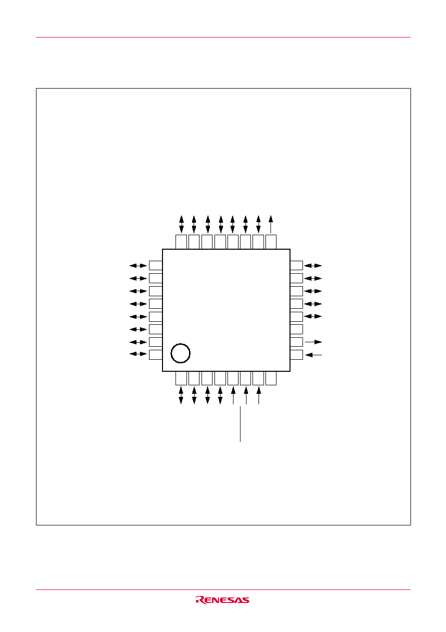
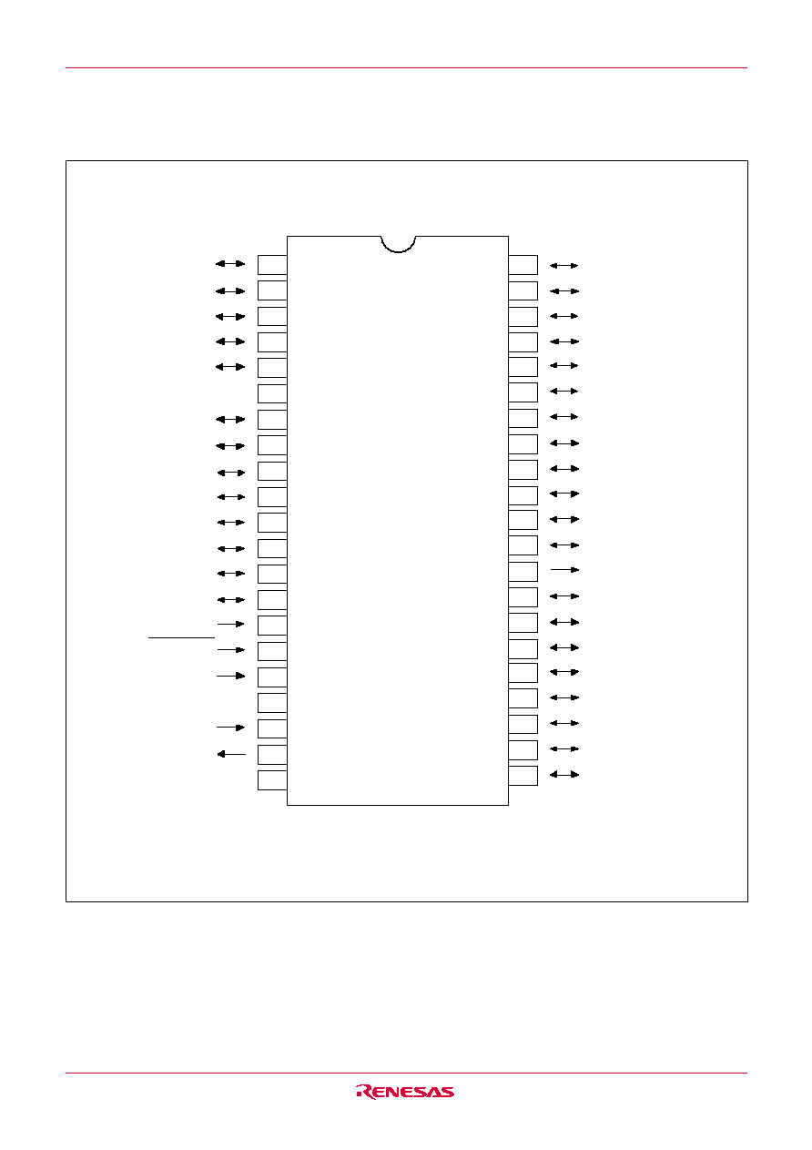
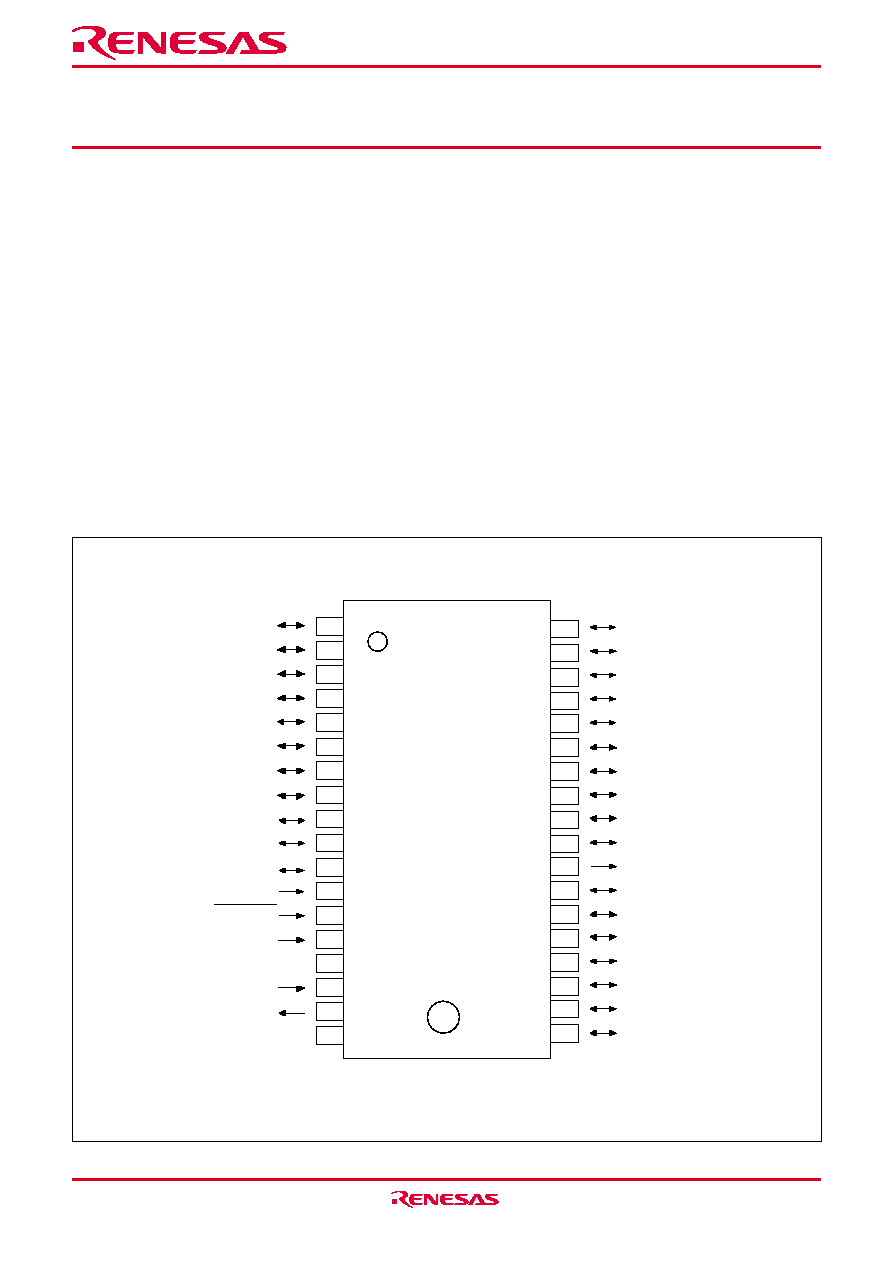
PIN CONFIGURATION (TOP VIEW)
Fig. 1 Pin configuration of M37534M4-XXXFP, M37534E8FP
Package type: 36P2R-A
10
1
2
3
4
6
7
8
9
11
12
14
15
16
5
13
17
18
36
35
34
33
31
30
26
25
24
23
22
21
20
19
32
27
29
28
P0
0
CNV
SS
X
OUT
X
IN
V
SS
P0
1
P0
2
P0
3
P0
4
P3
0
(LED
0
)
Vcc
V
REF
P0
5
P1
0
/R
X
D/D-
P2
6
/AN
6
P2
7
/AN
7
P1
1
/T
X
D/D+
P1
2
/S
CLK
P1
3
/S
DATA
P2
3
/AN
3
P2
2
/AN
2
P2
1
/AN
1
P2
0
/AN
0
P3
1
(LED
1
)
P3
7
/INT
0
P2
4
/AN
4
P2
5
/AN
5
P0
6
P0
7
USBV
REFOUT
RESET
M37534M4-XXXFP
M37534E8FP
P1
4
/CNTR
0
P3
5
(LED
5
)
P3
4
(LED
4
)
P3
3
(LED
3
)
P3
2
(LED
2
)