
Regarding the change of names mentioned in the document, such as Mitsubishi
Electric and Mitsubishi XX, to Renesas Technology Corp.
The semiconductor operations of Hitachi and Mitsubishi Electric were transferred to Renesas
Technology Corporation on April 1st 2003. These operations include microcomputer, logic, analog
and discrete devices, and memory chips other than DRAMs (flash memory, SRAMs etc.)
Accordingly, although Mitsubishi Electric, Mitsubishi Electric Corporation, Mitsubishi
Semiconductors, and other Mitsubishi brand names are mentioned in the document, these names
have in fact all been changed to Renesas Technology Corp. Thank you for your understanding.
Except for our corporate trademark, logo and corporate statement, no changes whatsoever have been
made to the contents of the document, and these changes do not constitute any alteration to the
contents of the document itself.
Note : Mitsubishi Electric will continue the business operations of high frequency & optical devices
and power devices.
Renesas Technology Corp.
Customer Support Dept.
April 1, 2003
To all our customers
Mar. 2002
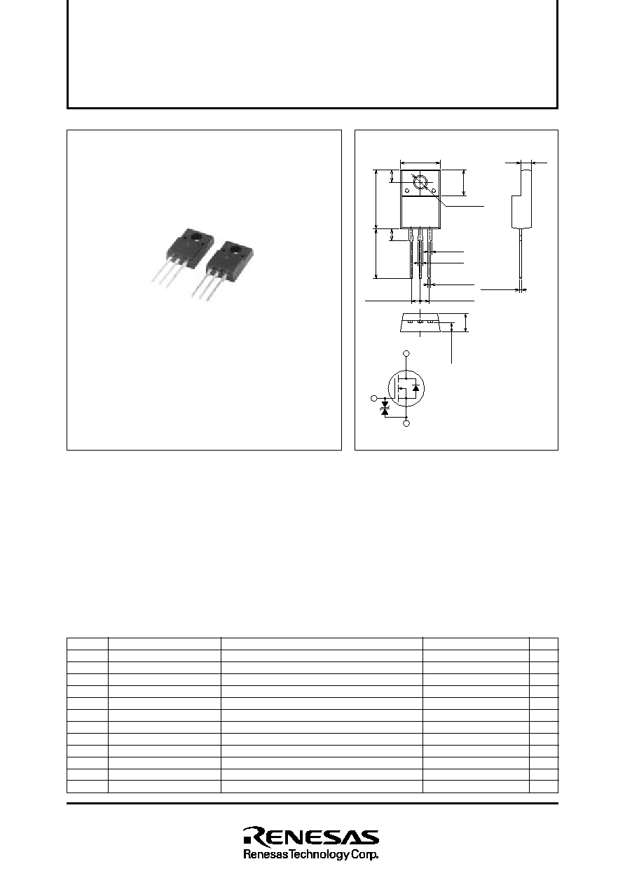
FS30KMJ-06F
OUTLINE DRAWING
Dimensions in mm
TO-220FN
MITSUBISHI Nch POWER MOSFET
FS30KMJ-06F
HIGH-SPEED SWITCHING USE
APPLICATION
Motor control, Lamp control, Solenoid control
DC-DC converter, etc.
V
V
A
A
A
A
A
W
∞
C
∞
C
V
g
60
±
20
30
120
30
30
120
25
≠55 ~ +150
≠55 ~ +150
2000
2.0
V
GS
= 0V
V
DS
= 0V
L = 10
µ
H
AC for 1 minute, Terminal to case
Typical value
Drain-source voltage
Gate-source voltage
Drain current
Drain current (Pulsed)
Avalanche current (Pulsed)
Source current
Source current (Pulsed)
Maximum power dissipation
Channel temperature
Storage temperature
Isolation voltage
Weight
V
DSS
V
GSS
I
D
I
DM
I
DA
I
S
I
SM
P
D
T
ch
T
stg
V
iso
--
Symbol
MAXIMUM RATINGS
(Tc = 25
∞
C)
Parameter
Conditions
Ratings
Unit
°
4V DRIVE
°
V
DSS ..................................................................................
60V
°
r
DS (ON) (MAX) ..............................................................
22m
°
I
D .........................................................................................
30A
°
Integrated Fast Recovery Diode (TYP.)
.............
50ns
15
±
0.3
14
±
0.5
10
±
0.3
2.8
±
0.2
3.2
±
0.2
1.1
±
0.2
1.1
±
0.2
0.75
±
0.15
2.54
±
0.25
2.54
±
0.25
2.6
±
0.2
4.5
±
0.2
0.75
±
0.15
3
±
0.3
3.6
±
0.3
6.5
±
0.3
GATE
DRAIN
SOURCE

Mar. 2002
V
(BR) DSS
V
(BR) GSS
I
DSS
I
GSS
V
GS (th)
r
DS (ON)
r
DS (ON)
V
DS (ON)
y
fs
C
iss
C
oss
C
rss
t
d (on)
t
r
t
d (off)
t
f
V
SD
R
th (ch-c)
t
rr
MITSUBISHI Nch POWER MOSFET
FS30KMJ-06F
HIGH-SPEED SWITCHING USE
V
V
µ
A
µ
A
V
m
m
V
S
pF
pF
pF
ns
ns
ns
ns
V
∞
C/W
ns
60
±
20
--
--
1.0
--
--
--
--
--
--
--
--
--
--
--
--
--
--
--
--
--
--
1.5
18
22
0.27
38
2600
385
200
13
70
240
100
1.0
--
50
--
--
100
±
10
2.0
22
28
0.33
--
--
--
--
--
--
--
--
1.5
5.00
--
ELECTRICAL CHARACTERISTICS
(Tch = 25
∞
C)
Drain-source breakdown voltage
Gate-source breakdown voltage
Drain-source leakage current
Gate-source leakage current
Gate-source threshold voltage
Drain-source on-state resistance
Drain-source on-state resistance
Drain-source on-state voltage
Forward transfer admittance
Input capacitance
Output capacitance
Reverse transfer capacitance
Turn-on delay time
Rise time
Turn-off delay time
Fall time
Source-drain voltage
Thermal resistance
Reverse recovery time
Symbol
Unit
Parameter
Test conditions
Limits
Min.
Typ.
Max.
I
D
= 1mA, V
GS
= 0V
I
G
=
±
100
µ
A, V
DS
= 0V
V
DS
= 60V, V
GS
= 0V
V
GS
=
±
20V, V
DS
= 0V
I
D
= 1mA, V
DS
= 10V
I
D
= 15A, V
GS
= 10V
I
D
= 15A, V
GS
= 4V
I
D
= 15A, V
GS
= 10V
I
D
= 15A, V
DS
= 10V
V
DS
= 10V, V
GS
= 0V, f = 1MHz
V
DD
= 30V, I
D
= 15A, V
GS
= 10V, R
GEN
= R
GS
= 50
I
S
= 15A, V
GS
= 0V
Channel to case
I
S
= 30A, dis/dt = ≠100A/
µ
s