
Rev.1.00, Aug.20.2004, page 1 of 6
FX6ASJ-03
High-Speed Switching Use
Pch Power MOS FET
REJ03G0247-0100
Rev.1.00
Aug.20.2004
Features
∑
Drive voltage : 4 V
∑
V
DSS
: ≠ 30 V
∑
r
DS(ON) (max)
: 0.29
∑
I
D
: ≠ 6 A
∑
Recovery Time of the Integrated Fast Recovery Diode (TYP.) : 40 ns
Outline
MP-3A
1
3
2
4
1. Gate
2. Drain
3. Source
4. Drain
1
2, 4
3
Applications
Motor control, lamp control, solenoid control, DC-DC converters, etc.
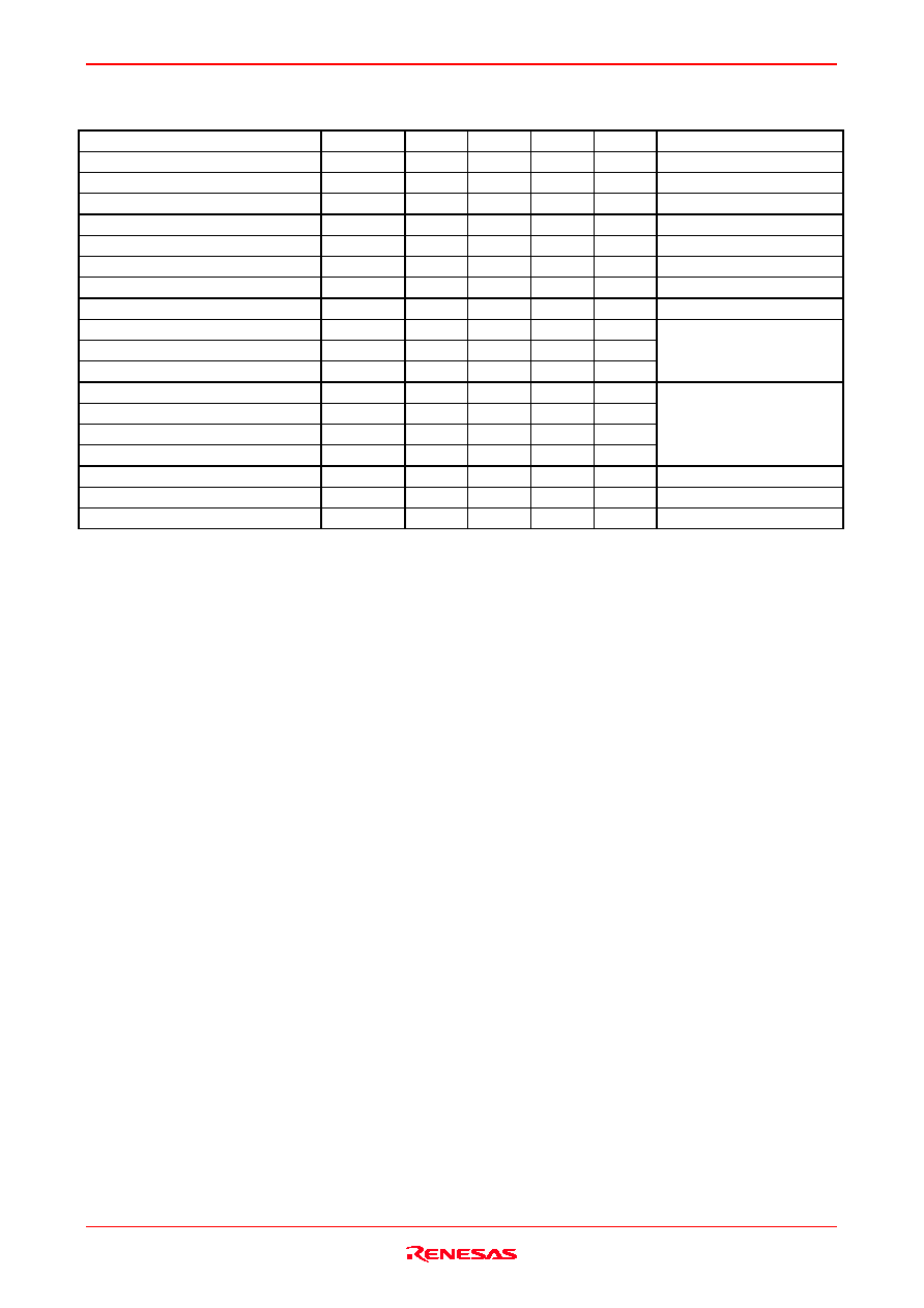
Maximum Ratings
(Tc = 25∞C)
Parameter
Symbol
Ratings
Unit
Conditions
Drain-source voltage
V
DSS
≠30
V
V
GS
= 0 V
Gate-source voltage
V
GSS
±
20
V
V
DS
= 0 V
Drain current
I
D
≠6
A
Drain current (Pulsed)
I
DM
≠24
A
Avalanche current (Pulsed)
I
DA
≠6
A
L = 30
µ
H
Source current
I
S
≠6
A
Source current (Pulsed)
I
SM
≠24
A
Maximum power dissipation
P
D
20
W
Channel temperature
Tch
≠ 55 to +150
∞
C
Storage temperature
Tstg
≠ 55 to +150
∞
C
Mass
--
0.32
g
Typical value
FX6ASJ-03
Rev.1.00, Aug.20.2004, page 2 of 6
Electrical Characteristics
(Tch = 25∞C)
Parameter
Symbol
Min.
Typ.
Max.
Unit
Test conditions
Drain-source breakdown voltage
V
(BR)DSS
≠30
--
--
V
I
D
= ≠1 mA, V
GS
= 0 V
Gate-source leakage current
I
GSS
--
--
±
0.1
µ
A
V
GS
=
±
20 V, V
DS
= 0 V
Drain-source leakage current
I
DSS
--
--
≠0.1
mA
V
DS
= ≠30 V, V
GS
= 0 V
Gate-source threshold voltage
V
GS(th)
≠1.3
≠1.8
≠2.3
V
I
D
= ≠1 mA, V
DS
= ≠10 V
Drain-source on-state resistance
r
DS(ON)
--
0.23
0.29
I
D
= ≠3 A, V
GS
= ≠10 V
Drain-source on-state resistance
r
DS(ON)
--
0.46
0.62
I
D
= ≠1 A, V
GS
= ≠ 4 V
Drain-source on-state voltage
V
DS(ON)
--
≠ 0.69
≠ 0.87
V
I
D
= ≠3 A, V
GS
= ≠10 V
Forward transfer admittance
| y
fs
|
--
2.6
--
S
I
D
= ≠3 A, V
DS
= ≠ 5 V
Input capacitance
Ciss
--
550
--
pF
Output capacitance
Coss
--
165
--
pF
Reverse transfer capacitance
Crss
--
45
--
pF
V
DS
= ≠10 V, V
GS
= 0 V,
f = 1MHz
Turn-on delay time
t
d(on)
--
9
--
ns
Rise time
t
r
--
14
--
ns
Turn-off delay time
t
d(off)
--
32
--
ns
Fall time
t
f
--
14
--
ns
V
DD
= ≠15 V, I
D
= ≠3 A,
V
GS
= ≠10 V,
R
GEN
= R
GS
= 50
Source-drain voltage
V
SD
--
≠1.0
≠1.5
V
I
S
= ≠3 A, V
GS
= 0 V
Thermal resistance
Rth(ch-c)
--
--
6.25
∞
C/W
Channel to case
Reverse recovery time
t
rr
--
40
--
ns
I
S
= ≠3 A, dis/dt = 50 A/
µ
s
FX6ASJ-03
Rev.1.00, Aug.20.2004, page 3 of 6
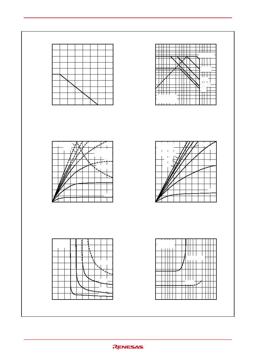
Performance Curves
Drain Power Dissipation Derating Curve
Case Temperature Tc (∞C)
Drain Power Dissipation P
D
(W)
Maximum Safe Operating Area
Drain-Source Voltage V
DS
(V)
Drain Current I
D
(A)
0
8
16
24
32
40
0
200
50
100
150
≠
10
≠1
≠
10
0
≠2
≠3
≠5
≠7
≠2
≠3
≠5
≠7
≠
10
2
≠
10
1
≠2
≠3
≠5
≠7
≠
10
0
≠10
1
≠10
2
≠2 ≠3 ≠5 ≠7
≠2 ≠3 ≠5 ≠7
≠2 ≠3 ≠5 ≠7
≠2
tw = 10
µs
100
µs
1ms
10ms
DC
Tc = 25∞C
Single Pulse
Output Characteristics (Typical)
Drain Current I
D
(A)
Drain-Source Voltage V
DS
(V)
Output Characteristics (Typical)
Drain Current I
D
(A)
Drain-Source Voltage V
DS
(V)
On-State Voltage vs.
Gate-Source Voltage (Typical)
Gate-Source Voltage V
GS
(V)
Drain-Source On-State Voltage V
DS(ON)
(V)
On-State Resistance vs.
Drain Current (Typical)
Drain Current I
D
(A)
Drain-Source On-State Resistance r
DS(ON)
(m
)
0
≠
2
≠
4
≠
6
≠
8
≠10
≠1.0
≠2.0
≠3.0
≠
4.0
≠
5.0
0
≠1.0
≠
2.0
≠
3.0
≠
4.0
≠
5.0
≠
0.4
≠
0.8
≠1.2
≠1.6
≠2.0
0
0
≠
7V
P
D
= 20W
Tc = 25∞C
Pulse Test
≠
5V
≠
3V
≠
4V
≠
6V
≠
5V
≠
3V
≠
4V
Tc = 25∞C
Pulse Test
≠
8V
V
GS
= ≠10V
≠
8V
V
GS
= ≠10V
≠
7V
≠
6V
0
0.2
0.4
0.6
0.8
1.0
≠10
≠1
≠2
≠10
0
≠3 ≠5 ≠7
≠2
≠10
1
≠3 ≠5 ≠7
≠2
≠10
2
≠3 ≠5 ≠7
V
GS
= ≠
4V
≠10V
Tc = 25∞C
Pulse Test
0
≠1.0
≠
2.0
≠
3.0
≠
4.0
≠
5.0
0
≠
2
≠
4
≠
6
≠
8
≠10
≠
6A
≠
3A
≠
1A
I
D
= ≠10A
Tc = 25∞C
Pulse Test

FX6ASJ-03
Rev.1.00, Aug.20.2004, page 4 of 6
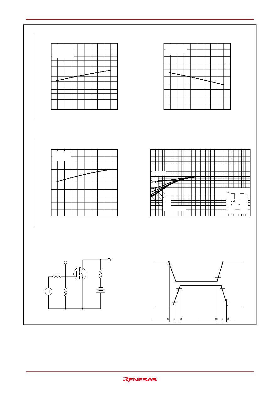
Transfer Characteristics (Typical)
Gate-Source Voltage V
GS
(V)
Drain Current I
D
(A)
Forward Transfer Admittance vs.
Drain Current (Typical)
Drain Current I
D
(A)
Forward Transfer Admittance | y
fs
| (S)
≠10
≠1
≠10
0
≠2 ≠3
≠5 ≠7
≠2 ≠3
≠5
≠10
1
≠7
10
0
2
3
5
7
10
1
2
3
5
7
V
DS
= ≠
5V
Pulse Test
0
≠
2
≠
4
≠
6
≠
8
≠10
0
≠
2
≠
4
≠
6
≠
8
≠10
Tc = 25∞C
V
DS
= ≠10V
Pulse Test
Switching Characteristics (Typical)
Drain-Source Voltage V
DS
(V)
Capacitance vs.
Drain-Source Voltage (Typical)
Drain Current I
D
(A)
Capacitance (pF)
Switching Time (ns)
Gate-Source Voltage vs.
Gate Charge (Typical)
Gate Charge Qg (nC)
Gate-Source Voltage V
GS
(V)
Source-Drain Diode Forward
Characteristics (Typical)
Source-Drain Voltage V
SD
(V)
Source Current I
S
(A)
≠10
0
≠3 ≠5≠7
≠2≠3 ≠5≠7
≠10
1
≠2≠3
≠2≠3
≠5≠7
≠10
2
10
3
10
4
2
3
5
7
10
2
2
3
5
7
2
3
5
7
Ciss
Coss
Crss
Tch = 25∞C
f = 1MHz
V
GS
= 0V
≠10
≠1
≠10
0
≠10
1
≠2 ≠3
≠5 ≠7
≠2 ≠3
≠5 ≠7
10
1
2
3
5
7
10
2
2
3
5
7
10
0
td(off)
td(on)
tf
tr
Tch = 25∞C
V
DD
= ≠15V
V
GS
= ≠10V
R
GEN
= R
GS
= 50
0
≠
2
≠
4
≠
6
≠
8
≠10
0
4
8
12
16
20
Tch = 25∞C
I
D
= ≠
6A
0
≠
4
≠
8
≠12
≠16
≠20
0
≠
0.4
≠
0.8
≠1.2
≠1.6
≠2.0
V
GS
= 0V
Pulse Test
75∞C
125∞C
Tc = 25∞C
V
DS
= ≠10V
≠
20V
≠
25V
Tc = 125∞C
75∞C
25∞C
FX6ASJ-03
Rev.1.00, Aug.20.2004, page 5 of 6
Channel Temperature Tch (∞C)
Drain-Source On-State Resistance r
DS(ON)
(t∞C)
Threshold Voltage vs.
Channel Temperature (Typical)
Gate-Source Threshold Voltage V
GS(th)
(V)
On-State Resistance vs.
Channel Temperature (Typical)
Drain-Source On-State Resistance r
DS(ON)
(25∞C)
Channel Temperature Tch (∞C)
0
≠
0.8
≠1.6
≠
2.4
≠
3.2
≠
4.0
≠50
0
50
100
150
V
DS
= ≠10V
I
D
= ≠1mA
10
≠1
10
0
2
3
5
7
10
1
2
3
5
7
≠50
0
50
100
150
V
GS
= ≠10V
I
D
= 1/2 I
D
Pulse Test
Transient Thermal Impedance Characteristics
Channel Temperature Tch (∞C)
Breakdown Voltage vs.
Channel Temperature (Typical)
Pulse Width tw (s)
Transient Thermal Impedance Zth(ch≠c) (∞C/W)
Drain-Source Breakdown Voltage V
(BR)DSS
(t∞C)
Drain-Source Breakdown Voltage V
(BR)DSS
(25∞C)
Switching Time Measurement Circuit
Switching Waveform
0.4
0.6
0.8
1.0
1.2
1.4
≠50
0
50
100
150
V
GS
= 0V
I
D
= ≠1mA
10
≠1
10
0
2
3
5
7
10
1
2
3
5
7
10
2
2
3
5
7
10
≠4
2 3 5 7
2 3 5 7
2 3 5 7
2 3 5 7
10
0
2 3 5 7
10
1
2 3 5 7
10
2
10
≠3
10
≠2
10
≠1
D = 1.0
0.5
0.2
0.1
0.05
0.02
Single Pulse
R
L
V
DD
R
GEN
R
GS
Vin Monitor
D.U.T.
tr
td(on)
Vin
90%
90%
10%
10%
Vout
td(off)
Vout
Monitor
90%
10%
tf
P
DM
tw
D =
T
tw
T
0.01