 | –≠–ª–µ–∫—Ç—Ä–æ–Ω–Ω—ã–π –∫–æ–º–ø–æ–Ω–µ–Ω—Ç: H5N3011P | –°–∫–∞—á–∞—Ç—å:  PDF PDF  ZIP ZIP |
Rev.2.00, Aug.05.2004, page 1 of 6
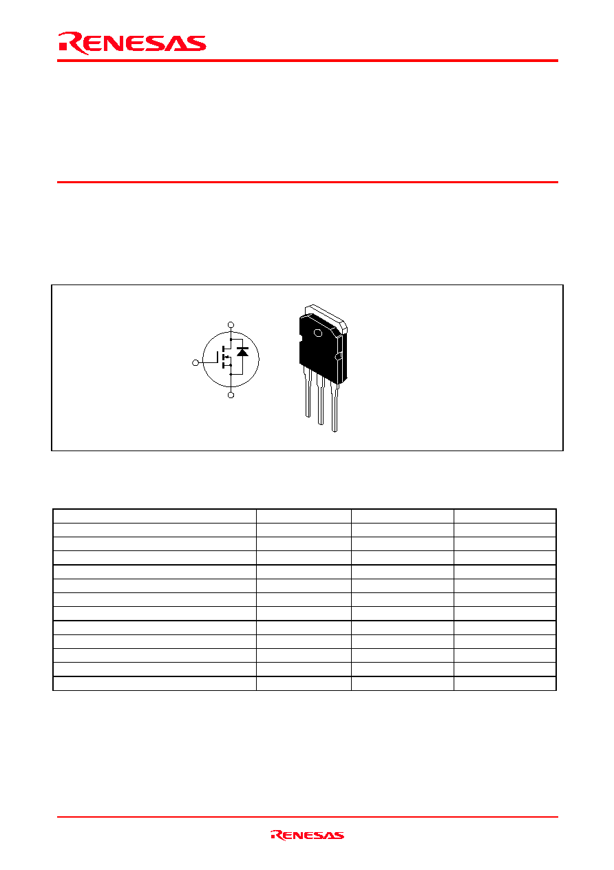
H5N3011P
Silicon N Channel MOS FET
High Speed Power Switching
REJ03G0385-0200
Rev.2.00
Aug.05.2004
Features
∑
Low on-resistance
∑
Low leakage current
∑
High speed switching
Outline
TO-3P
1
2
3
D
S
G
1. Gate
2. Drain (Flange)
3. Source
Absolute Maximum Ratings
(Ta = 25∞C)
Item
Symbol
Ratings
Unit
Drain to Source voltage
V
DSS
300
V
Gate to Source voltage
V
GSS
±30
V
Drain current
I
D
88
A
Drain peak current
I
D (pulse)
Note1
176
A
Body-Drain diode reverse Drain current
I
DR
88
A
Body-Drain diode reverse Drain peak current
I
DR (pulse)
Note1
176
A
Avalanche current
I
AP
Note3
30
A
Avalanche energy
E
AR
Note3
54
mJ
Channel dissipation
Pch
Note2
150
W
Channel to case thermal impedance
ch-c
0.833
∞
C/W
Channel temperature
Tch
150
∞
C
Storage temperature
Tstg
≠55 to +150
∞
C
Notes: 1. PW
10
µ
s, duty cycle
1%
2. Value at Tc = 25
∞
C
3. STch = 25
∞
C, Tch
150
∞
C

H5N3011P
Rev.2.00, Aug.05.2004, page 2 of 6
Electrical Characteristics
(Ta = 25∞C)
Item
Symbol
Min
Typ
Max
Unit
Test conditions
Drain to Source breakdown voltage
V
(BR)DSS
300
--
--
V
I
D
= 10 mA, V
GS
= 0
Zero Gate voltage Drain current
I
DSS
--
--
1
µ
A
V
DS
= 300 V, V
GS
= 0
Gate to Source leak current
I
GSS
--
--
±0.1
µ
A
V
GS
=
±
30 V, V
DS
= 0
Gate to Source cutoff voltage
V
GS(off)
3.0
--
4.5
V
V
DS
= 10 V, I
D
= 1 mA
Forward transfer admittance
|yfs|
33
56
--
S
I
D
= 44 A, V
DS
= 10 V
Note4
Static Drain to Source on state
resistance
R
DS(on)
--
0.042
0.048
I
D
= 44 A, V
GS
= 10 V
Note4
Input capacitance
Ciss
--
5000
--
pF
Output capacitance
Coss
--
640
--
pF
Reverse transfer capacitance
Crss
--
65
--
pF
V
DS
= 25 V
V
GS
= 0
f = 1 MHz
Turn-on delay time
t
d(on)
--
60
--
ns
Rise time
t
r
--
370
--
ns
Turn-off delay time
t
d(off)
--
200
--
ns
Fall time
t
f
--
280
--
ns
I
D
= 44 A
V
GS
= 10 V
R
L
= 3.4
Rg = 10
Total Gate charge
Qg
--
95
--
nC
Gate to Source charge
Qgs
--
25
--
nC
Gate to Drain charge
Qgd
--
40
--
nC
V
DD
= 240 V
V
GS
= 10 V
I
D
= 88 A
Body-Drain diode forward voltage
V
DF
--
1.0
1.5
V
I
F
= 88 A, V
GS
= 0
Note4
Body-Drain diode reverse recovery time
trr
--
260
--
ns
Body-Drain diode reverse recovery
charge
Qrr
--
2.5
--
µ
C
I
F
= 88 A, V
GS
= 0
diF/dt = 100 A/
µ
s
Notes: 4. Pulse test

H5N3011P
Rev.2.00, Aug.05.2004, page 3 of 6
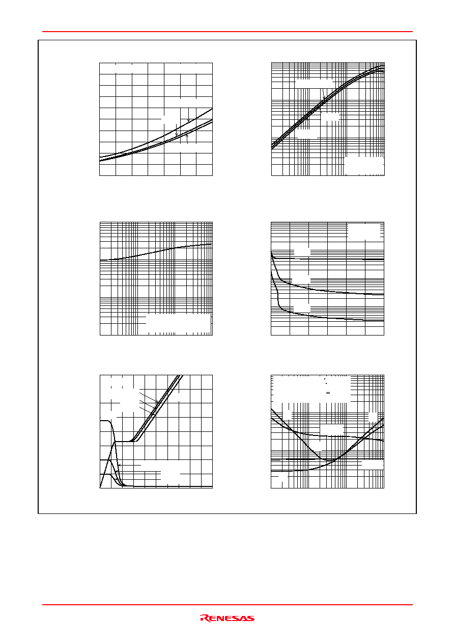
Main Characteristics
200
150
100
50
0
50
100
150
200
100
80
60
40
20
0
4
8
12
16
20
100
80
60
40
20
0
2
4
6
8
10
V
GS
= 5 V
6 V
Tc = 75
∞C
25
∞C
-25∞C
Channel Dissipation Pch (W)
Case Temperature Tc (
∞C)
Power vs. Temperature Derating
Drain to Source Voltage V
DS
(V)
Drain Current I
D
(A)
Typical Output Characteristics
Pulse Test
Gate to Source Voltage V
GS
(V)
Drain Current I
D
(A)
Typical Transfer Characteristics
V
DS
= 10 V
Pulse Test
8 V
10 V
6
4
2
0
4
8
12
16
20
1
30
100
3
10
300
1000
0.02
0.01
0.005
0.1
0.05
0.002
0.001
Gate to Source Voltage V
GS
(V)
Drain to Source Saturation Voltage vs.
Gate to Source Voltage
Drain to Source Saturation Voltage
V
DS(on)
(V)
Drain Current I
D
(A)
Drain to Source on State Resistance
R
DS(on)
(
)
Static Drain to Source on State Resistance
vs. Drain Current
8
I
D
= 88 A
44 A
20 A
Pulse Test
V
GS
= 10 V, 15 V
Pulse Test
5.5 V
300
100
30
10
3
1
1
3
10
30
300
1000
0.3
0.01
0.1
0.03
1000
Drain to Source Voltage V
DS
(V)
Drain Current I
D
(A)
Maximum Safe Operation Area
100
Ta = 25
∞C
100
µs
1 ms
10
µs
Operation in
this area is
limited by R
DS(on)
PW = 10 ms
(1shot)
DC Operation
(Tc = 25
∞C)
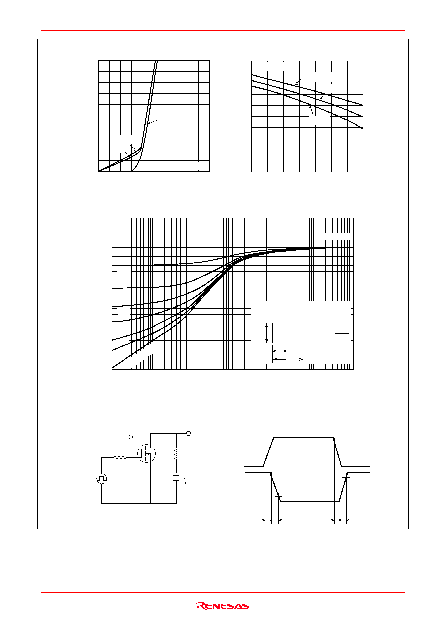
H5N3011P
Rev.2.00, Aug.05.2004, page 4 of 6
0.2
0.16
0.12
0.08
0.04
-25 0
25
50
75
100 125
150
0
0.3
0.1
3
30
100
100
30
10
3
1
0.3
0.1
1
10
Case Temperature Tc (
∞C)
Static Drain to Source on State Resistance
R
DS(on)
(
)
Static Drain to Source on State Resistance
vs. Temperature
Drain Current I
D
(A)
Forward Transfer Admittance vs.
Drain Current
Forward Transfer Admittance |yfs| (S)
25
∞C
Tc =
-25∞C
75
∞C
V
DS
= 10 V
Pulse Test
V
GS
= 10 V
Pulse Test
I
D
= 88 A
20 A
44 A
0.1
0.3
1
3
10
30
100
1000
200
500
100
20
50
10
2
5
1
0
50
100
150
30000
10000
100000
1000
3000
400
0
16
300
12
200
8
100
4
40
80
120
160
200
0
10000
1000
10
100
0.1
0.3
1
3
10
30
100
300
100
30
10
V
GS
= 0
f = 1 MHz
Ciss
Coss
Crss
I
D
= 88 A
V
DS
V
GS
Reverse Drain Current I
DR
(A)
Reverse Recovery Time trr (ns)
Body-Drain Diode Reverse
Recovery Time
Capacitance C (pF)
Drain to Source Voltage V
DS
(V)
Typical Capacitance vs.
Drain to Source Voltage
Gate Charge Qg (nC)
Drain to Source Voltage V
DS
(V)
Gate to Source Voltage V
GS
(V)
Dynamic Input Characteristics
Drain Current I
D
(A)
Switching Time t (ns)
Switching Characteristics
di / dt = 100 A /
µs
V
GS
= 0, Ta = 25
∞C
V
DD
= 240 V
100 V
50 V
tr
td(on)
td(off)
tf
V
GS
= 10 V, V
DD
= 150 V
PW = 5
µs, duty < 1 %
R
G
= 10
tr
tf
V
DD
= 50 V
100 V
240 V
H5N3011P
Rev.2.00, Aug.05.2004, page 5 of 6
0
0.4
0.8
1.2
1.6
2.0
100
40
V
GS
= 0 V
10 V
Source to Drain Voltage V
SD
(V)
Reverse Drain Current vs.
Source to Drain Voltage
Reverse Drain Current I
DR
(A)
Pulse Test
5
4
3
2
1
-25
0
50
100
150
25
125
75
0
Case Temperature Tc (
∞C)
Gate to Source Cutoff Voltage
vs. Case Temperature
Gate to Source Cutoff Voltage
V
GS(off)
(V)
V
DS
= 10 V
Vin Monitor
D.U.T.
Vin
10 V
R
L
V
= 150 V
DD
tr
td(on)
Vin
90%
90%
10%
10%
Vout
td(off)
Vout
Monitor
10
90%
10%
t
f
Switching Time Test Circuit
Waveform
5 V
I
D
= 10 mA
1 mA
0.1 mA
20
60
80
3
1
0.3
0.1
0.03
0.01
10
µ
100
µ
1 m
10 m
100 m
1
10
DM
P
PW
T
D =
PW
T
ch ≠ c(t) = s (t) ∑ ch ≠ c
ch ≠ c = 0.833
∞
C/W, Tc = 25
∞
C
Tc = 25
∞
C
D = 1
0.5
0.2
0.1
0.05
0.02
0.01
1shot pulse
Pulse Width PW (s)
Normalized Transient Thermal Impedance
s (t)
Normalized Transient Thermal Impedance vs. Pulse Width