Regarding the change of names mentioned in the document, such as Hitachi
Electric and Hitachi XX, to Renesas Technology Corp.
The semiconductor operations of Mitsubishi Electric and Hitachi were transferred to Renesas
Technology Corporation on April 1st 2003. These operations include microcomputer, logic, analog
and discrete devices, and memory chips other than DRAMs (flash memory, SRAMs etc.)
Accordingly, although Hitachi, Hitachi, Ltd., Hitachi Semiconductors, and other Hitachi brand
names are mentioned in the document, these names have in fact all been changed to Renesas
Technology Corp. Thank you for your understanding. Except for our corporate trademark, logo and
corporate statement, no changes whatsoever have been made to the contents of the document, and
these changes do not constitute any alteration to the contents of the document itself.
Renesas Technology Home Page: http://www.renesas.com
Renesas Technology Corp.
Customer Support Dept.
April 1, 2003
To all our customers

Cautions
Keep safety first in your circuit designs!
1. Renesas Technology Corporation puts the maximum effort into making semiconductor products better
and more reliable, but there is always the possibility that trouble may occur with them. Trouble with
semiconductors may lead to personal injury, fire or property damage.
Remember to give due consideration to safety when making your circuit designs, with appropriate
measures such as (i) placement of substitutive, auxiliary circuits, (ii) use of nonflammable material or
(iii) prevention against any malfunction or mishap.
Notes regarding these materials
1. These materials are intended as a reference to assist our customers in the selection of the Renesas
Technology Corporation product best suited to the customer's application; they do not convey any
license under any intellectual property rights, or any other rights, belonging to Renesas Technology
Corporation or a third party.
2. Renesas Technology Corporation assumes no responsibility for any damage, or infringement of any
third-party's rights, originating in the use of any product data, diagrams, charts, programs, algorithms, or
circuit application examples contained in these materials.
3. All information contained in these materials, including product data, diagrams, charts, programs and
algorithms represents information on products at the time of publication of these materials, and are
subject to change by Renesas Technology Corporation without notice due to product improvements or
other reasons. It is therefore recommended that customers contact Renesas Technology Corporation
or an authorized Renesas Technology Corporation product distributor for the latest product information
before purchasing a product listed herein.
The information described here may contain technical inaccuracies or typographical errors.
Renesas Technology Corporation assumes no responsibility for any damage, liability, or other loss
rising from these inaccuracies or errors.
Please also pay attention to information published by Renesas Technology Corporation by various
means, including the Renesas Technology Corporation Semiconductor home page
(http://www.renesas.com).
4. When using any or all of the information contained in these materials, including product data, diagrams,
charts, programs, and algorithms, please be sure to evaluate all information as a total system before
making a final decision on the applicability of the information and products. Renesas Technology
Corporation assumes no responsibility for any damage, liability or other loss resulting from the
information contained herein.
5. Renesas Technology Corporation semiconductors are not designed or manufactured for use in a device
or system that is used under circumstances in which human life is potentially at stake. Please contact
Renesas Technology Corporation or an authorized Renesas Technology Corporation product distributor
when considering the use of a product contained herein for any specific purposes, such as apparatus or
systems for transportation, vehicular, medical, aerospace, nuclear, or undersea repeater use.
6. The prior written approval of Renesas Technology Corporation is necessary to reprint or reproduce in
whole or in part these materials.
7. If these products or technologies are subject to the Japanese export control restrictions, they must be
exported under a license from the Japanese government and cannot be imported into a country other
than the approved destination.
Any diversion or reexport contrary to the export control laws and regulations of Japan and/or the
country of destination is prohibited.
8. Please contact Renesas Technology Corporation for further details on these materials or the products
contained therein.
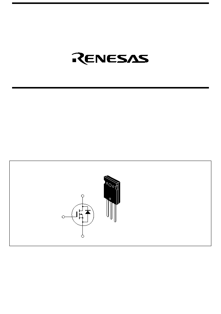
H5N5005PL
Silicon N Channel MOS FET
High Speed Power Switching
ADE-208-1382 (Z)
Target Specification 1st. Edition
Mar. 2001
Features
∑
Low on-resistance: R
DS(on)
= 0.064
typ.
∑
Low leakage current: IDSS = 10
µ
A max (at VDS = 500 V)
∑
High speed switching: tf = 300 ns typ (at VGS = 10 V, VDD = 250 V, ID = 30 A)
∑
Low gate charge: Qg = 300 nC typ (at VDD = 400 V, VGS = 10 V, ID = 60 A)
∑
Avalanche ratings
∑
Built-in fast recovery diode: trr = 220 ns typ
Outline
TO-3PL
D
G
S
1
2
3
1. Gate
2. Drain (Flange)
3. Source
H5N5005PL
3
Electrical Characteristics (Ta = 25
∞
C)
Item
Symbol
Min
Typ
Max
Unit
Test Conditions
Drain to source breakdown
voltage
V
(BR)DSS
500
--
--
V
I
D
= 10 mA, V
GS
= 0
Gate to source leak current
I
GSS
--
--
±
0.1
µ
A
V
GS
=
±
30 V, V
DS
= 0
Zero gate voltage drain current
I
DSS
--
--
10
µ
A
V
DS
= 500 V, V
GS
= 0
Gate to source cutoff voltage
V
GS(off)
2.0
--
4.0
V
V
DS
= 10 V, I
D
= 1 mA
Static drain to source on state
resistance
R
DS(on)
--
0.064
0.075
I
D
= 30 A, V
GS
= 10 V
Note4
Forward transfer admittance
|y
fs
|
30
50
--
S
I
D
= 30 A, V
DS
= 10 V
Note4
Input capacitance
Ciss
--
10550
--
pF
V
DS
= 25 V
Output capacitance
Coss
--
1060
--
pF
V
GS
= 0
Reverse transfer capacitance
Crss
--
180
--
pF
f = 1 MHz
Turn-on delay time
td(on)
--
115
--
ns
I
D
= 30 A
Rise time
tr
--
380
--
ns
V
GS
= 10 V
Turn-off delay time
td(off)
--
560
--
ns
R
L
= 8.33
Fall time
tf
--
300
--
ns
Rg = 10
Total gate charge
Qg
--
300
--
nC
V
DD
= 400 V
Gate to source charge
Qgs
--
40
--
nC
V
GS
= 10 V
Gate to drain charge
Qgd
--
155
--
nC
I
D
= 60 A
Body-drain diode forward
voltage
V
DF
--
1.05
1.6
V
I
F
= 60 A, V
GS
= 0
Body-drain diode reverse
recovery time
trr
--
220
--
ns
I
F
= 60 A, V
GS
= 0
Body-drain diode reverse
recovery charge
Qrr
--
2.0
--
µ
C
diF/dt = 100 A/
µ
s
Note:
4. Pulse test