 | –≠–ª–µ–∫—Ç—Ä–æ–Ω–Ω—ã–π –∫–æ–º–ø–æ–Ω–µ–Ω—Ç: H7N0308AB | –°–∫–∞—á–∞—Ç—å:  PDF PDF  ZIP ZIP |
H7N0308AB
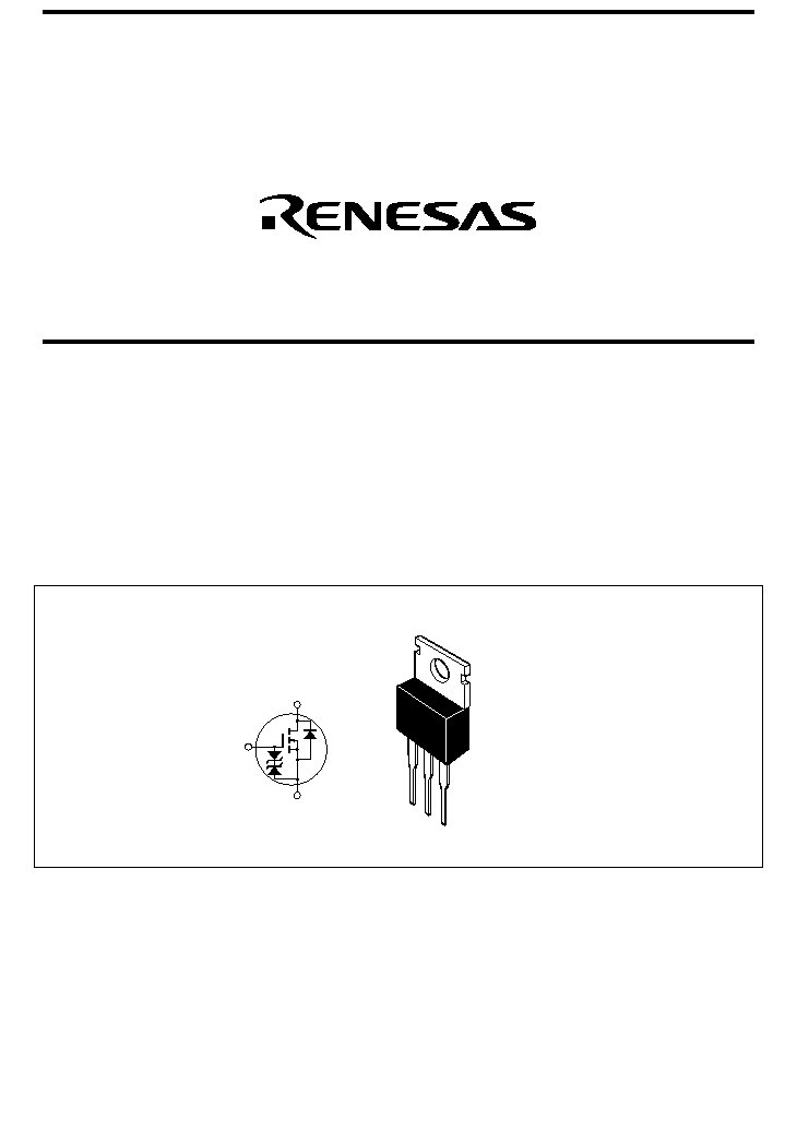
Silicon N Channel MOS FET
High Speed Power Switching
ADE-208-1569B(Z)
3rd. Edition
Aug. 2002
Features
∑ Low on-resistance
∑ R
DS(on)
= 3.8 m
typ.
∑ Low drive current
∑ 4.5 V gate drive device can be driven from 5 V source
Outline
TO-220AB
1
2
3
1. Gate
2. Drain
(Frange)
3. Source
D
G
S

H7N0308AB
Rev.2, Aug. 2002, page 2 of 9
Absolute Maximum Ratings
(Ta = 25∞C)
Item Symbol
Ratings
Unit
Drain to source voltage
V
DSS
30 V
Gate to source voltage
V
GSS
±20 V
Drain current
I
D
70
A
Drain peak current
I
D(pulse)
Note 1
280
A
Body-drain diode reverse drain current I
DR
70 A
Channel dissipation
Pch
Note 2
100
W
Channel to Case Thermal Impedance
ch-c
1.25 ∞C/W
Channel
temperature Tch 150 ∞C
Storage temperature
Tstg
≠55 to +150
∞C
Notes: 1. PW
10 µs, duty cycle 1 %
2. Value at Tc = 25∞C
H7N0308AB
Rev.2, Aug. 2002, page 3 of 9
Electrical Characteristics
(Ta = 25∞C)
Item Symbol
Min
Typ
Max
Unit
Test
Conditions
Drain to source breakdown voltage V
(BR)DSS
30
--
-- V I
D
= 10 mA, V
GS
= 0
Gate to source breakdown voltage V
(BR)GSS
±20 --
--
I
G
= ±100
µA, V
DS
= 0
Gate to source leak current
I
GSS
--
-- ±10
µA V
GS
= ±16 V, V
DS
= 0
Zero gate voltage drain current
I
DSS
--
-- 10
µA V
DS
= 30 V, V
GS
= 0
Gate to source cutoff voltage
V
GS(off)
1.0 -- 2.5 V I
D
= 1 mA, V
DS
= 10 V
Note 1
Static drain to source on state
R
DS(on)
-- 3.8 4.8 m
I
D
= 35 A, V
GS
= 10 V
Note 1
resistance
-- 6.0 8.5 m
I
D
= 35 A, V
GS
= 4.5 V
Note 1
Forward transfer admittance
|y
fs
| 54 90 -- S I
D
= 35 A, V
DS
= 10 V
Note 1
Input capacitance
Ciss
-- 3350
-- pF V
DS
= 10 V
Output capacitance
Coss
-- 840
-- pF V
GS
= 0
Reverse transfer capacitance
Crss
-- 480
--
pF
f = 1MHz
Total gate charge
Qg
-- 52 -- nc V
DD
= 10 V
Gate to source charge
Qgs
-- 11 -- nc V
GS
= 10 V
Gate to drain charge
Qgd
-- 10 -- nc I
D
= 70 A
Turn-on delay time
t
d(on)
-- 30 -- ns V
GS
= 10 V, I
D
= 35 A
Rise time
t
r
-- 370
-- ns R
L
=0.29
Turn-off delay time
t
d(off)
-- 80 -- ns R
g
=4.7
Fall time
t
f
-- 27 -- ns
Body≠drain diode forward voltage
V
DF
-- 0.93
-- V I
F
= 70 A, V
GS
= 0
Body≠drain diode reverse recovery
time
t
rr
-- 60 -- ns I
F
= 70 A, V
GS
= 0
diF/ dt =50 A/µs
Notes: 1. Pulse test

H7N0308AB
Rev.2, Aug. 2002, page 4 of 9
Main Characteristics
Drain to Source Voltage V
DS
(V)
Drain Current I
D
(A)
Maximum Safe Operation Area
Drain to Source Voltage V
DS
(V)
Drain Current I
D
(A)
Typical Output Characteristics
Gate to Source Voltage V
GS
(V)
Drain Current I
D
(A)
Typical Transfer Characteristics
100
80
60
40
20
0
2
4
6
8
10
100
80
60
40
20
0
1
2
3
4
5
Tc = 75
∞C
25
∞C
-25
∞C
100
10
1
0.1
0.01
0.1
0.3
1
3
10
30
100
V = 10 V
Pulse Test
DS
500
Tc = 25
∞C
1 shot Pulse
PW = 1
0 ms
10
µs
100
µs
Operation in
this area is
limited by R
DS(on)
DC Operation
1 ms
V = 2.5 V
GS
10V
4.5 V
3.5 V
Pulse Test
3 V
160
120
80
40
0
50
100
150
200
Channel Dissipation Pch (W)
Case Temperature Tc (
∞C)
Power vs. Temperature Derating

H7N0308AB
Rev.2, Aug. 2002, page 5 of 9
Gate to Source Voltage V
GS
(V)
Drain to Source Voltage V
DS(on)
(mV)
Drain to Source Saturation Voltage vs.
Gate to Source Voltage
Drain Current I
D
(A)
Drain to Source On State Resistance
R
DS(on)
(m
)
Static Drain to Source on State Resistance
vs. Drain Current
Case Temperature Tc (
∞C)
Drain to Source On State Resistance
R
DS(on)
(m
)
Static Drain to Source on State Resistance
vs. Temperature
Forward Transfer Admittance |yfs| (S)
Drain Current I
D
(A)
Forward Transfer Admittance vs.
Drain Current
500
400
300
200
100
0
4
8
12
16
20
3
1
30
10
0.3
0.1
3
30
300
12
10
8
6
4
2
-25
0
25
50
75
100 125
150
0
Pulse Test
I = 50 A
D
10 A
20 A
1
10
100
1000
100
V = 4.5 V
GS
10 V
Pulse Test
I = 50 A
D
I = 10 A, 20 A
D
10 A, 20 A, 50 A
V = 4.5 V
GS
10 V
Pulse Test
3
30
1
10
100
10
100
300
1000
30
1
3
Tc = -25
∞C
DS
V = 10 V
Pulse Test
75
∞C
25
∞C