 | –≠–ª–µ–∫—Ç—Ä–æ–Ω–Ω—ã–π –∫–æ–º–ø–æ–Ω–µ–Ω—Ç: HA16142P | –°–∫–∞—á–∞—Ç—å:  PDF PDF  ZIP ZIP |

Regarding the change of names mentioned in the document, such as Hitachi
Electric and Hitachi XX, to Renesas Technology Corp.
The semiconductor operations of Mitsubishi Electric and Hitachi were transferred to Renesas
Technology Corporation on April 1st 2003. These operations include microcomputer, logic, analog
and discrete devices, and memory chips other than DRAMs (flash memory, SRAMs etc.)
Accordingly, although Hitachi, Hitachi, Ltd., Hitachi Semiconductors, and other Hitachi brand
names are mentioned in the document, these names have in fact all been changed to Renesas
Technology Corp. Thank you for your understanding. Except for our corporate trademark, logo and
corporate statement, no changes whatsoever have been made to the contents of the document, and
these changes do not constitute any alteration to the contents of the document itself.
Renesas Technology Home Page: http://www.renesas.com
Renesas Technology Corp.
Customer Support Dept.
April 1, 2003
To all our customers

Cautions
Keep safety first in your circuit designs!
1. Renesas Technology Corporation puts the maximum effort into making semiconductor products better
and more reliable, but there is always the possibility that trouble may occur with them. Trouble with
semiconductors may lead to personal injury, fire or property damage.
Remember to give due consideration to safety when making your circuit designs, with appropriate
measures such as (i) placement of substitutive, auxiliary circuits, (ii) use of nonflammable material or
(iii) prevention against any malfunction or mishap.
Notes regarding these materials
1. These materials are intended as a reference to assist our customers in the selection of the Renesas
Technology Corporation product best suited to the customer's application; they do not convey any
license under any intellectual property rights, or any other rights, belonging to Renesas Technology
Corporation or a third party.
2. Renesas Technology Corporation assumes no responsibility for any damage, or infringement of any
third-party's rights, originating in the use of any product data, diagrams, charts, programs, algorithms, or
circuit application examples contained in these materials.
3. All information contained in these materials, including product data, diagrams, charts, programs and
algorithms represents information on products at the time of publication of these materials, and are
subject to change by Renesas Technology Corporation without notice due to product improvements or
other reasons. It is therefore recommended that customers contact Renesas Technology Corporation
or an authorized Renesas Technology Corporation product distributor for the latest product information
before purchasing a product listed herein.
The information described here may contain technical inaccuracies or typographical errors.
Renesas Technology Corporation assumes no responsibility for any damage, liability, or other loss
rising from these inaccuracies or errors.
Please also pay attention to information published by Renesas Technology Corporation by various
means, including the Renesas Technology Corporation Semiconductor home page
(http://www.renesas.com).
4. When using any or all of the information contained in these materials, including product data, diagrams,
charts, programs, and algorithms, please be sure to evaluate all information as a total system before
making a final decision on the applicability of the information and products. Renesas Technology
Corporation assumes no responsibility for any damage, liability or other loss resulting from the
information contained herein.
5. Renesas Technology Corporation semiconductors are not designed or manufactured for use in a device
or system that is used under circumstances in which human life is potentially at stake. Please contact
Renesas Technology Corporation or an authorized Renesas Technology Corporation product distributor
when considering the use of a product contained herein for any specific purposes, such as apparatus or
systems for transportation, vehicular, medical, aerospace, nuclear, or undersea repeater use.
6. The prior written approval of Renesas Technology Corporation is necessary to reprint or reproduce in
whole or in part these materials.
7. If these products or technologies are subject to the Japanese export control restrictions, they must be
exported under a license from the Japanese government and cannot be imported into a country other
than the approved destination.
Any diversion or reexport contrary to the export control laws and regulations of Japan and/or the
country of destination is prohibited.
8. Please contact Renesas Technology Corporation for further details on these materials or the products
contained therein.

HA16141P/FP, HA16142P/FP
PFC and PWM Controller
ADE-204-036D (Z)
Preliminary
Rev.4
Sep. 2001
Description
The HA16141P/FP and the HA16142P/FP are power supply controller ICs combining an AC-DC converter
switching controllers for power factor correction and off-line power supply switching controllers. PFC
(Power factor correction) section employs average current mode PWM and off-line power supply control
section employs peak current mode PWM.
The HA16142P/FP is the change version of HA16141P/FP's PWM maximum on duty cycle.
The PFC operation can be turned on and off by external control signal. Use of this on/off function makes it
possible to disable PFC operation at a low line voltage, or to perform remote control operation from the
transformer secondary side. The PFC power supply boosted output voltage is not only fed to an error
amplifier input signal but also fed to as the boost voltage monitor circuit.
PG signal is put out if the boost
voltage is out-of-spec.
The PWM controller, which begins operation at the same time as release of the IC's UVLO (under-voltage
lockout) is suitable for auxiliary power supply use in a multi-output power supply system.
Features
∑ Synchronized PFC and PWM timing
∑ Self oscillation with fixed frequency
PFC : 100 kHz (
±15 %)
PWM : 200 kHz (
±15 %)
∑ PFC function on/off control
∑ PFC boosted output voltage monitor
∑ High-output current gate drivers
PFC driver peak current :
±1.5 A typ.
PWM driver peak current :
±1.0 A typ.
∑ PWM maximum on duty cycle
72% min (HA16141P/FP)
49.5% max (HA16142P/FP)
HA16141P/FP, HA16142P/FP
Rev.4, Sep. 2001, page 2 of 2
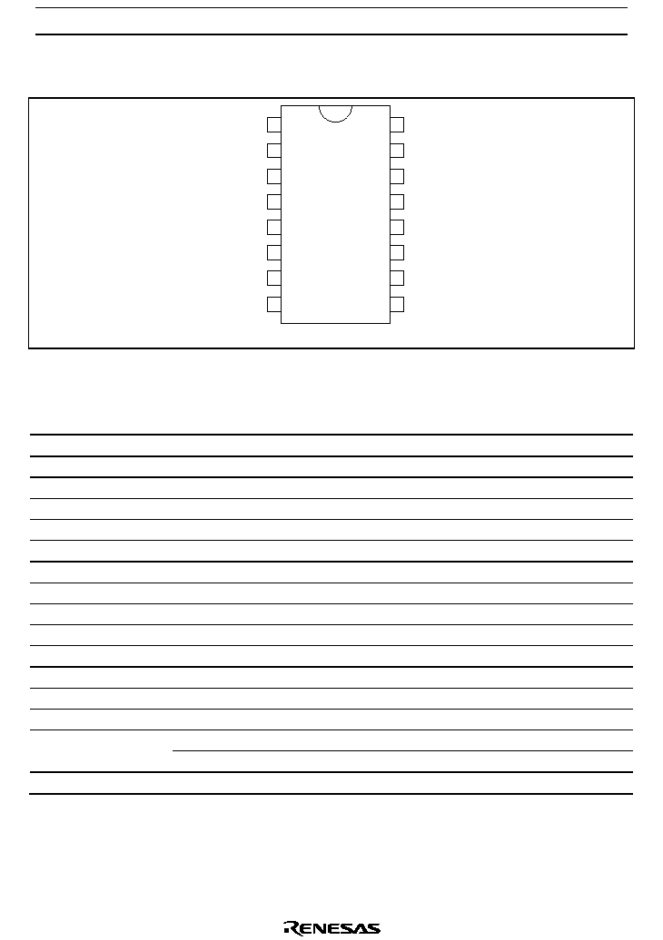
Pin Arrangement
(Top view)
1
2
3
4
5
6
7
8
PWM-CS
PWM-EO
O.C
PFC-EO
TIM
PFC-FB
IAC
PFC-ON
16
15
14
13
12
11
10
9
GND
PWM-OUT
PFC-OUT
VCC
VREF
2/
CAO
PFC-CS
Pin Description
Pin No.
Symbol
Function
1 GND
Ground
2
PWM-OUT
Power MOS FET driver output (PWM control)
3
PFC-OUT
Power MOS FET driver output (PFC control)
4 VCC
Supply
voltage
5 VREF
Reference
voltage
6
PG
Power Good signal output (open-drain output)
7
CAO
Average current control error amp. output
8
PFC-CS
PFC control current sense signal input
9
PFC-ON
PFC function on/off signal input
10
IAC
Multiplier reference current input
11
PFC-FB
PFC control error amp. input
12
TIM
Overcurrent timer time setting
13
PFC-EO
PFC control error amp. output
14
O.C
Overcurrent detector signal input
PWM control error amp. output (photocoupler input also possible) (HA16141 only)
15 PWM-EO
PWM control feedback voltage signal input (HA16142 only)
16
PWM-CS
PWM control current sense signal input
HA16141P/FP, HA16142P/FP
Rev.4, Sep. 2001, page 3 of 3
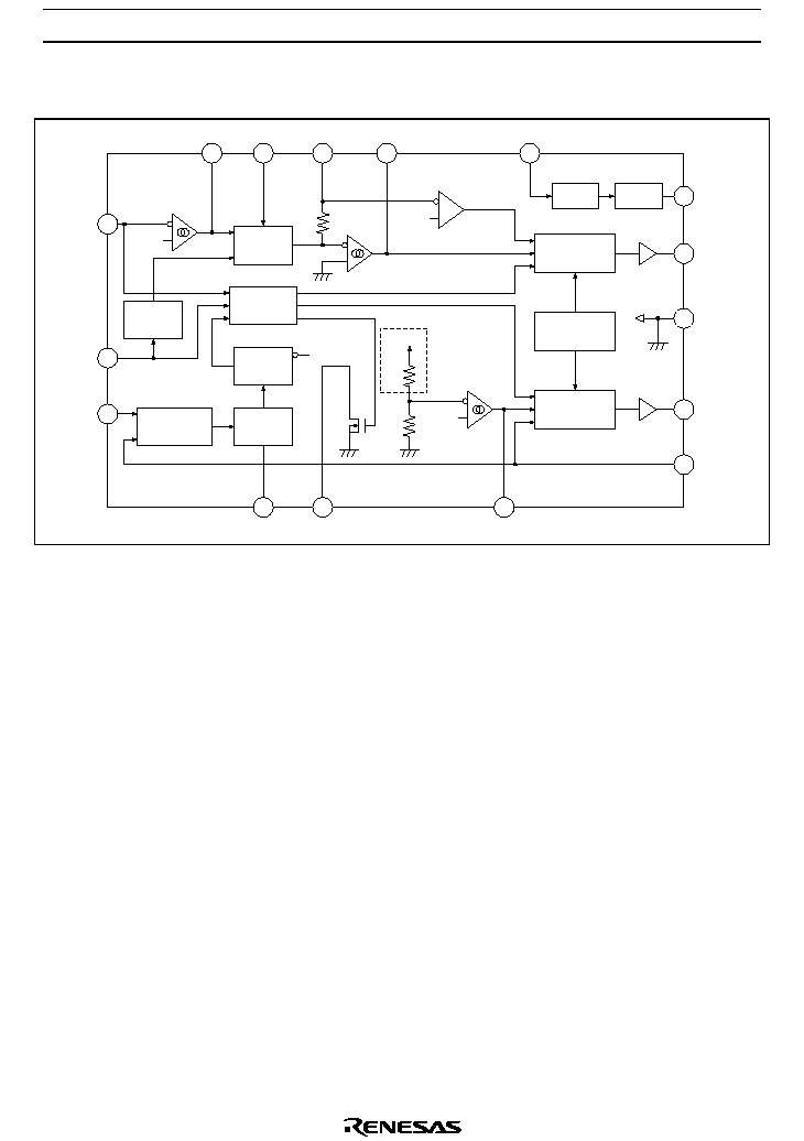
Block Diagram
13
11
2.5V
-0.5V
PFC-FB
14
O.C
9
PFC-ON
PFC-EO
PFC-V
AMP
PWM-V
AMP
PFC-C
AMP
PFC-C
LIMIT
7
CAO
4
5 VREF
1 GND
2 PWM-OUT
16 PWM-CS
3 PFC-OUT
VCC
10
IAC
2.5V
100kHz
±1.5A
200kHz
Multiplier
Integrator
LATCH
RES
VCC
VCC
5R
2.7k
PFC/PWM
Supervisor
±1.0A
Over
Current Det.
Gain
Selector
8
PFC-CS
PFC Control
UVLO
VREF
Oscillator
PWM Control
R
12
6
TIM
15
PWM-EO
2/
HA16141 only