Regarding the change of names mentioned in the document, such as Hitachi
Electric and Hitachi XX, to Renesas Technology Corp.
The semiconductor operations of Mitsubishi Electric and Hitachi were transferred to Renesas
Technology Corporation on April 1st 2003. These operations include microcomputer, logic, analog
and discrete devices, and memory chips other than DRAMs (flash memory, SRAMs etc.)
Accordingly, although Hitachi, Hitachi, Ltd., Hitachi Semiconductors, and other Hitachi brand
names are mentioned in the document, these names have in fact all been changed to Renesas
Technology Corp. Thank you for your understanding. Except for our corporate trademark, logo and
corporate statement, no changes whatsoever have been made to the contents of the document, and
these changes do not constitute any alteration to the contents of the document itself.
Renesas Technology Home Page: http://www.renesas.com
Renesas Technology Corp.
Customer Support Dept.
April 1, 2003
To all our customers

Cautions
Keep safety first in your circuit designs!
1. Renesas Technology Corporation puts the maximum effort into making semiconductor products better
and more reliable, but there is always the possibility that trouble may occur with them. Trouble with
semiconductors may lead to personal injury, fire or property damage.
Remember to give due consideration to safety when making your circuit designs, with appropriate
measures such as (i) placement of substitutive, auxiliary circuits, (ii) use of nonflammable material or
(iii) prevention against any malfunction or mishap.
Notes regarding these materials
1. These materials are intended as a reference to assist our customers in the selection of the Renesas
Technology Corporation product best suited to the customer's application; they do not convey any
license under any intellectual property rights, or any other rights, belonging to Renesas Technology
Corporation or a third party.
2. Renesas Technology Corporation assumes no responsibility for any damage, or infringement of any
third-party's rights, originating in the use of any product data, diagrams, charts, programs, algorithms, or
circuit application examples contained in these materials.
3. All information contained in these materials, including product data, diagrams, charts, programs and
algorithms represents information on products at the time of publication of these materials, and are
subject to change by Renesas Technology Corporation without notice due to product improvements or
other reasons. It is therefore recommended that customers contact Renesas Technology Corporation
or an authorized Renesas Technology Corporation product distributor for the latest product information
before purchasing a product listed herein.
The information described here may contain technical inaccuracies or typographical errors.
Renesas Technology Corporation assumes no responsibility for any damage, liability, or other loss
rising from these inaccuracies or errors.
Please also pay attention to information published by Renesas Technology Corporation by various
means, including the Renesas Technology Corporation Semiconductor home page
(http://www.renesas.com).
4. When using any or all of the information contained in these materials, including product data, diagrams,
charts, programs, and algorithms, please be sure to evaluate all information as a total system before
making a final decision on the applicability of the information and products. Renesas Technology
Corporation assumes no responsibility for any damage, liability or other loss resulting from the
information contained herein.
5. Renesas Technology Corporation semiconductors are not designed or manufactured for use in a device
or system that is used under circumstances in which human life is potentially at stake. Please contact
Renesas Technology Corporation or an authorized Renesas Technology Corporation product distributor
when considering the use of a product contained herein for any specific purposes, such as apparatus or
systems for transportation, vehicular, medical, aerospace, nuclear, or undersea repeater use.
6. The prior written approval of Renesas Technology Corporation is necessary to reprint or reproduce in
whole or in part these materials.
7. If these products or technologies are subject to the Japanese export control restrictions, they must be
exported under a license from the Japanese government and cannot be imported into a country other
than the approved destination.
Any diversion or reexport contrary to the export control laws and regulations of Japan and/or the
country of destination is prohibited.
8. Please contact Renesas Technology Corporation for further details on these materials or the products
contained therein.

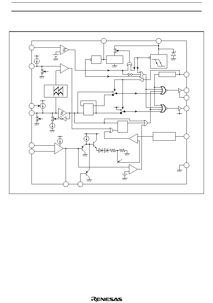
HA16150T/P
High-Speed Current Mode
Push-Pull PWM Control IC
ADE-204-071A (Z)
Rev.1
Sep. 2002
Description
The HA16150 is a high-speed current mode PWM control IC with push-pull dual outputs, suitable for high-
reliability, high-efficiency, high-mounting-density isolated DC-DC converter and high-output AC-DC
converter control.
The HA16150 can be used in various applications, including push-pull converters and half-bridge, double-
forward, and single-forward applications.
The HA16150 incorporates 180-degree phase-inverted push-pull dual outputs, and directly drives a power
MOS FET. Operation at a maximum of 1 MHz is possible on an oscillator reference frequency.
The package lineup comprises an ultra-thin surface-mount TSSOP-16 suitable for slim communication
system modules, and a general-purpose insertion DILP-6 suitable for characteristics evaluation.
Features
<Maximum Ratings>
∑ Supply voltage Vcc: 20 V
∑ Peak output current Ipk-out: ±1.0 A
∑ Operating junction temperature Tjopr: ≠40∞C to +125∞C
<Electrical Characteristics>
∑ VREF output voltage VREF: 5.0 V ± 1%
∑ UVLO start threshold VH: 9.3 V ± 0.7 V
∑ UVLO shutdown threshold VL: 8.3 V ± 0.7 V
∑ Operating current Icc: 4 mA typ.
∑ Standby current Is: 150 µA typ.
<Functions>
∑ Soft start (one external timing capacitance)
∑ Remote on/off control
∑ Independent dead band time adjustment
∑ Current limiter adjustment (set drooping characteristic adjustment)
∑ Push-pull/single-end output switching
∑ Package lineup: TSSOP-16/DILP-16

HA16150T/P
Rev.1, Sep. 2002, page 2 of 23
Pin Arrangement
(Top view)
1
2
3
4
5
6
7
8
VREF
REMOTE
VCC
OUT2
PGND
OUT1
TDB
SGND
16
15
14
13
12
11
10
9
INP
INM
EOUT
CSLIM
CS
RT
CT
SS
Pin Functions
Pin No.
Pin Name
Pin Function
1
INP
Error amplifier non-inverted (+) input
2
INM
Error amplifier inverted (-) input
3 EOUT Error
amplifier
output
4
CSLIM
Current limiter level adjustment
5
CS
Current sense signal input
6
RT
Operating frequency setting resistance connection
7
CT
Operating frequency setting capacitance connection
8
SS
Soft start time setting timing capacitance connection
9
SGND
Small signal system ground
10
TDB
Dead band time setting timing capacitance connection
11
OUT1
Power MOS FET driver output 1
12
PGND
Power system ground
13
OUT2
Power MOS FET driver output 2
14 VCC
Supply
voltage
15 REMOTE Remote
on/off
control
16 VREF
Reference
voltage