 | –≠–ª–µ–∫—Ç—Ä–æ–Ω–Ω—ã–π –∫–æ–º–ø–æ–Ω–µ–Ω—Ç: HA16163T | –°–∫–∞—á–∞—Ç—å:  PDF PDF  ZIP ZIP |
Rev.5.0, Mar.15.2004, page 1 of 29
HA16163T
Synchronous Phase Shift Full-Bridge Control IC
REJ03F0001-0500Z
Rev.5.0
Mar.15.2004
Features
∑ High frequency operation; oscillator frequency = 2 MHz max.
∑ Full-bridge phase-shift switching circuit with adjustable delay times
∑ Integrated secondary synchronous rectification control with adjustable delay times
∑ Three-level over current protection; pulse by pulse, timer Latch, one shot OCP
∑ Package: TSSOP-20
Application
∑ 48 V input isolated DC/DC converter
∑ Primary; Full-bridge circuit topology
∑ Secondary; current doubler or center-tapped rectification
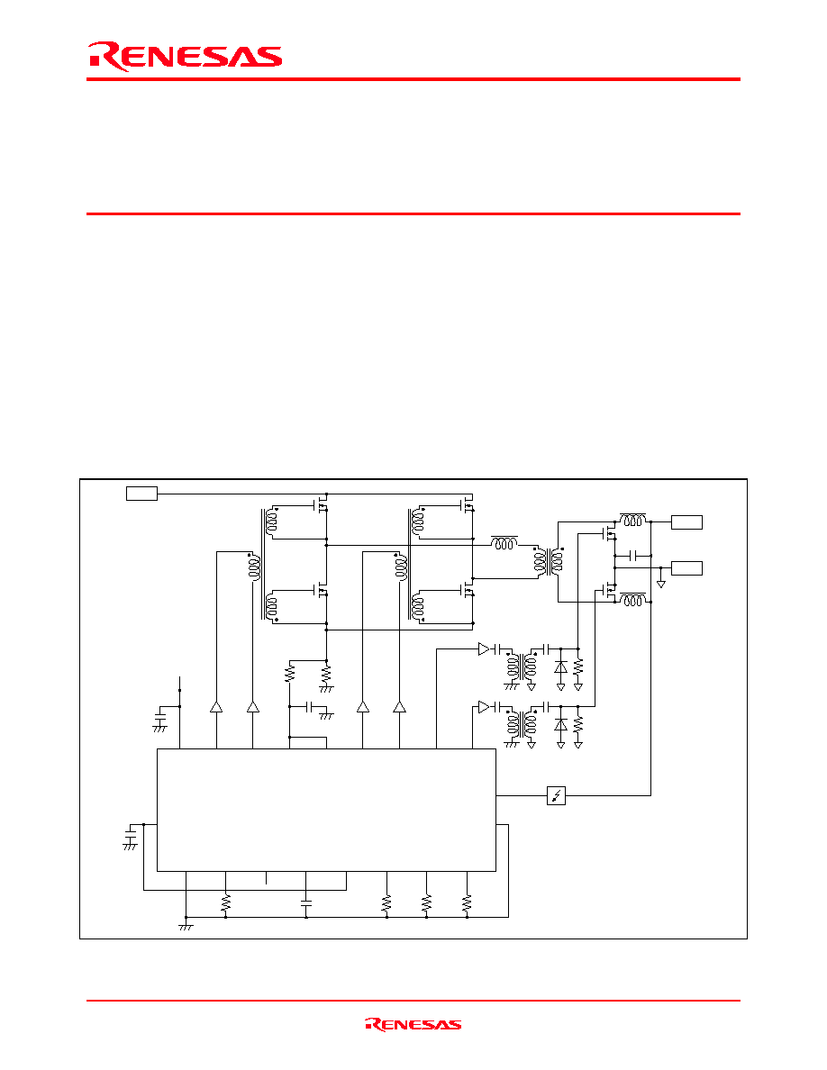
Illustrative Circuit
GND
RT
SYNC
SS
REMOTE
DELAY
-1
DELAY
-2
DELAY
-3
VREF
VCC
Vbias
OUT
-A
OUT
-B
CS
RAMP
OUT
-C
OUT
-D
OUT
-F
OUT
-E
FET
Driver
FET
Driver
FET
Driver
FET
Driver
FET Driver
Optical feedback circuitry
+48V
+
≠
FB
COMP
FET Driver
HA16163T
Rev.5.0, Mar.15.2004, page 2 of 29
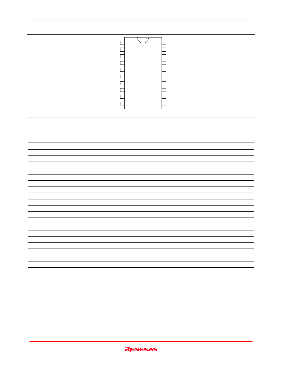
Pin Arrangement
(Top view)
2
3
4
5
6
7
8
RT
GND
OUT-A
OUT-B
OUT-C
OUT-D
OUT-E
OUT-F
VCC
VREF
20
19
18
17
16
15
14
13
9
12
11
1
SYNC
RAMP
CS
COMP
REMOTE
FB
SS
DELAY-1
DELAY-2
10
DELAY-3
Pin Functions
Pin No.
Pin Name
Pin Function
1
SYNC
Synchronization I/O for the oscillator
2
RAMP
Current sense signal input for the full-bridge control loop
3
CS
Current sense signal input for OCP
4 COMP Error
amplifier
output
5 REMOTE Remote
on/off
control
6
FB
Voltage feedback input
7
SS
Timing capacitor for both soft start and timer latch
8
DELAY-1
Delay time adjustor for the full-bridge control signal (OUT-A and B)
9
DELAY-2
Delay time adjustor for the full-bridge control signal (OUT-C and D)
10
DELAY-3
Delay time adjustor for the secondary control signal (OUT-E and F)
11
VREF
5 V/20 mA Output
12
VCC
IC power supply input
13
OUT-F
Secondary control signal
14
OUT-E
Secondary control signal
15
OUT-D
Full-bridge control signal
16
OUT-C
Full-bridge control signal
17
OUT-B
Full-bridge control signal
18
OUT-A
Full-bridge control signal
19
GND
Ground level for the IC
20
RT
Timing resistor for the oscillator

HA16163T
Rev.5.0, Mar.15.2004, page 3 of 29
Block Diagram
-
+
-
+
-
+
5V
Generator
Current Ref.
Generator
Start-up
counter
32 clock
ON: 1.417V
OFF: 1.333V
1.55V
1.46V
VREF
RES
Oscillator
Note that all switches in the block diagram are turned on when control signal is high.
REMOTE
-
+
FB
COMP
RAMP
RES
PULSE BY PULSE
VREF
Error Amp
SYNC. I/O
Comparator
RT
SYNC
VCC
UVL
L
UVLO
H
L
H
VREF
GOOD
VREF
OUT-A
OUT-B
DELAY-1
VREF
4V
Clamp Circuit
500
µ
Q
87
µ
A
10
µ
1.25V
0.4V
-
+
ONE SHOT
0.6V
SS
CS
GND
-
+
0.4V
20k
10k
SS IN
LOCKOUT
LIMIT IN
S
R
Q
VREF
GOOD
VREF
GOOD
Circuit Bias
Zero delay
S
R
Q
S
R
Q
DISCHARGE
FAULT
LOGIC
ONE PULSE
SEQ.
VREF
VREF
DELAY
DELAY
OUT-C
OUT-D
DELAY-2
VREF
VREF
DELAY
DELAY
OUT-E
OUT-F
DELAY-3
VREF
VREF
DELAY
DELAY
Zero Delay

HA16163T
Rev.5.0, Mar.15.2004, page 4 of 29
Absolute Maximum Ratings
(Ta = 25∞C)
Item Symbol
Rating
Unit
Note
Power supply voltage
Vcc
20
V
1
Peak output current
Ipk-out
±50
mA
2, 3
DC output current
Idc-out
±5
mA
3
VREF output current
Iref-out
≠20
mA
3
COMP sink current
Isink-comp
2
mA
3
DELAY set current
Iset-delay
0.3
mA
3
RT set current
Iset-rt
0.3
mA
3
VREF terminal voltage
Vter-ref
≠0.3 to 6
V
1, 4
Terminal group 1 voltage
Vter-1
≠0.3 to (Vref +0.3)
V
1, 5
Operating junction temperature
Tj-opr
≠40 to +125
∞C
6
Storage temperature
Tstg
≠55 to +150
∞C
Notes: 1. Rated voltages are with reference to the GND pin.
2. Shows the transient current when driving a capacitive load.
3. For rated currents, inflow to the IC is indicated by (+), and outflow by (≠).
4. VREF pin voltage must not exceed VCC pin voltage.
5. Terminal group 1 is defined the pins;
REMOTE, CS, RAMP, COMP, FB, SS, RT, SYNC, DELAY-1 to 3, OUT-A to F
6.
ja
228∞C/W Board condition; Glass epoxy 55 mm
◊
45 mm
◊
1.6 mm, 10% wiring density.

HA16163T
Rev.5.0, Mar.15.2004, page 5 of 29
Electrical Characteristics
(Ta = 25∞C, Vcc = 12 V, RT = 33 k
, Rdelay = 51 k, unless otherwise specified.)
Item Symbol
Min
Typ
Max
Unit
Test
Conditions
Start threshold
VH
9.0
9.8
10.6
V
Shutdown
threshold VL
7.3 7.9 8.5 V
UVLO hysteresis
dV
UVL
1.7 1.9 2.1 V
Start-up current
Is
--
90
150
µ
A Vcc
=
8.5V
Supply
Operating
current
Icc
-- 7 10 mA No
load
on
VREF
pin
Output
voltage
Vref
4.9 5.0 5.1 V
Line regulation
Vref-line
--
0
10
mV
Vcc = 10V to 16V
Load regulation
Vref-load
--
6
20
mV
Iref = ≠1mA to ≠20mA
VREF
Temperature stability
dVref/dTa
--
±80 *
1
--
ppm/∞C
Ta = ≠40 to 105∞C
Oscillator frequency
fosc
--
960 *
1
--
kHz
Switching frequency
fsw
412
480
547
kHz
Measured on OUT-A, -B
Line stability
fsw-line
≠1.5
0
1.5
%
Vcc = 10V to 16V
Temperature stability
dfsw/dTa
--
±0.1 *
1
--
%/∞C
Ta = ≠40 to 105∞C
Oscillator
RT voltage
V
RT
2.5 2.7 2.9 V
Input threshold
V
TH-SYNC
2.5 2.85 3.2 V
Output high
V
OH-SYNC
3.5
4.0
--
V
R
SYNC
= 33k
to GND
Output low
V
OL-SYNC
--
0.05 0.15 V
R
SYNC
= 33k
to VREF
Minimum input pulse
T
I-MIN
50 -- -- ns
SYNC
Output pulse width
T
O-SYNC
-- 500
-- ns
On threshold voltage
V
ON
1.374 1.417 1.460 V
Off threshold voltage
V
OFF
1.293 1.333 1.373 V
Remote
Input bias current
I
REMOTE
0
0.4 2
µ
A REMOTE
=
2V
FB input voltage
V
FB
1.225 1.250 1.275 V
FB and COMP are shorted
FB input current
I
FB
≠1.0
0
1.0
µ
A FB
=
1.25V
Open-loop DC gain
Av
--
80 *
1
-- dB
Unity gain bandwidth
BW
--
2 *
1
-- MHz
Output source current
I
SOURCE
≠610 ≠430 ≠350
µ
A
FB = 0.75V, COMP = 2V
Output sink current
I
SINK
2.0
6.5
--
mA
FB = 1.75V, COMP = 2V
Output high voltage
V
OH-EO
3.7
3.9
--
V
FB = 0.75V, COMP; open
Output low voltage
V
OL-EO
--
0.1
0.4
V
FB = 1.75V, COMP; open
Error
amplifier
Output clamp voltage *
2
V
CLAMP-EO
≠0.16
≠0.07
0.0
V
FB = 0.75V, COMP; open
SS = 1V
Notes: 1. Reference values for design. Not 100% tested in production.
2.
V
CLAMP-EO
= V
COMP
≠ SS voltage (1V)