Regarding the change of names mentioned in the document, such as Hitachi
Electric and Hitachi XX, to Renesas Technology Corp.
The semiconductor operations of Mitsubishi Electric and Hitachi were transferred to Renesas
Technology Corporation on April 1st 2003. These operations include microcomputer, logic, analog
and discrete devices, and memory chips other than DRAMs (flash memory, SRAMs etc.)
Accordingly, although Hitachi, Hitachi, Ltd., Hitachi Semiconductors, and other Hitachi brand
names are mentioned in the document, these names have in fact all been changed to Renesas
Technology Corp. Thank you for your understanding. Except for our corporate trademark, logo and
corporate statement, no changes whatsoever have been made to the contents of the document, and
these changes do not constitute any alteration to the contents of the document itself.
Renesas Technology Home Page: http://www.renesas.com
Renesas Technology Corp.
Customer Support Dept.
April 1, 2003
To all our customers

Cautions
Keep safety first in your circuit designs!
1. Renesas Technology Corporation puts the maximum effort into making semiconductor products better
and more reliable, but there is always the possibility that trouble may occur with them. Trouble with
semiconductors may lead to personal injury, fire or property damage.
Remember to give due consideration to safety when making your circuit designs, with appropriate
measures such as (i) placement of substitutive, auxiliary circuits, (ii) use of nonflammable material or
(iii) prevention against any malfunction or mishap.
Notes regarding these materials
1. These materials are intended as a reference to assist our customers in the selection of the Renesas
Technology Corporation product best suited to the customer's application; they do not convey any
license under any intellectual property rights, or any other rights, belonging to Renesas Technology
Corporation or a third party.
2. Renesas Technology Corporation assumes no responsibility for any damage, or infringement of any
third-party's rights, originating in the use of any product data, diagrams, charts, programs, algorithms, or
circuit application examples contained in these materials.
3. All information contained in these materials, including product data, diagrams, charts, programs and
algorithms represents information on products at the time of publication of these materials, and are
subject to change by Renesas Technology Corporation without notice due to product improvements or
other reasons. It is therefore recommended that customers contact Renesas Technology Corporation
or an authorized Renesas Technology Corporation product distributor for the latest product information
before purchasing a product listed herein.
The information described here may contain technical inaccuracies or typographical errors.
Renesas Technology Corporation assumes no responsibility for any damage, liability, or other loss
rising from these inaccuracies or errors.
Please also pay attention to information published by Renesas Technology Corporation by various
means, including the Renesas Technology Corporation Semiconductor home page
(http://www.renesas.com).
4. When using any or all of the information contained in these materials, including product data, diagrams,
charts, programs, and algorithms, please be sure to evaluate all information as a total system before
making a final decision on the applicability of the information and products. Renesas Technology
Corporation assumes no responsibility for any damage, liability or other loss resulting from the
information contained herein.
5. Renesas Technology Corporation semiconductors are not designed or manufactured for use in a device
or system that is used under circumstances in which human life is potentially at stake. Please contact
Renesas Technology Corporation or an authorized Renesas Technology Corporation product distributor
when considering the use of a product contained herein for any specific purposes, such as apparatus or
systems for transportation, vehicular, medical, aerospace, nuclear, or undersea repeater use.
6. The prior written approval of Renesas Technology Corporation is necessary to reprint or reproduce in
whole or in part these materials.
7. If these products or technologies are subject to the Japanese export control restrictions, they must be
exported under a license from the Japanese government and cannot be imported into a country other
than the approved destination.
Any diversion or reexport contrary to the export control laws and regulations of Japan and/or the
country of destination is prohibited.
8. Please contact Renesas Technology Corporation for further details on these materials or the products
contained therein.

HA17904A Series
Dual Operational Amplifier
ADE-204-069 (Z)
Rev.0
May 2001
Description
HA17904A series are dual operational amplifier that provide high gain and internal phase compensation,
with single power supply. They can be widely applied to control equipments and to general use.
Features
∑ Wide range of supply voltage, and single power supply used
∑ Wide range of common mode voltage, and possible to operate with an input about 0 V, and output
around 0 V is available
∑ Frequency characteristics and input bias current are temperature compensated
∑ Low electro-magnetic susceptibility level
Output Offset Voltage vs. Input Interference
Measurement Condition
Output offset voltage
(arb. unit)
5.0
4.0
3.0
2.0
1.0
0
-1.0
100E+3
1E+6
10E+6
100E+6
1E+9
10E+9
Input RF frequency (Hz)
HA17904A series
HA17904 series
Rs
-
+
Rs
0.01
µ
Vin
-10 dBm
RF signal source
(for quasi-RF noise)
Vcc = +7.5 V
Vee =
-7.5 V
Rf
Rf
Vout
(= 100
Vio)
V
_
Improve-
ment
HA17904A Series
Rev.0, May 2001, page 2 of 9
Ordering Information
Type No.
Application
Package
HA17904APS Industrial
use DP-8B
HA17904AFP
FP-8D
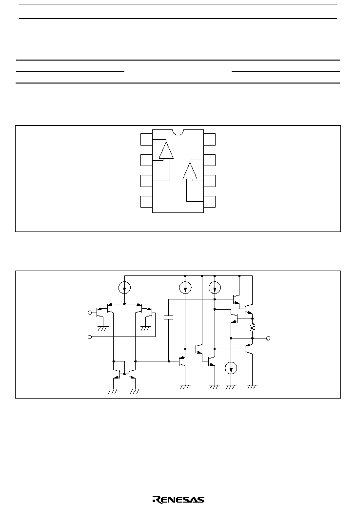
Pin Arrangement
- +
Vout1
Vin(
-)1
Vin(+)1
GND
V
CC
Vout2
Vin(
-)2
Vin(+)2
+
-
8
7
6
5
1
2
3
4
(Top View)
1
2
Circuit Schematic (1/2)
Q
1
Q
4
Q
2
Q
3
Q
5
Q
6
Q
7
Q
13
Q
12
Q
11
Q
10
Q
8
Q
9
Vout
R
1
Vin(+)
Vin(
-)
C
HA17904A Series
Rev.0, May 2001, page 3 of 9
Absolute Maximum Ratings
(Ta = 25
∞C)
Ratings
Item
Symbol
HA17904APS HA17904AFP
Unit
Supply voltage
V
CC
32 32 V
Sink current
Isink
50
50
mA
Power dissipation
P
T
570
*
1
385
*
2
mW
Common mode input voltage
V
CM
-0.3 to V
CC
-0.3 to V
CC
V
Differential input voltage
Vin (diff)
±V
CC
±V
CC
V
Operating temperature
Topr
-40 to +85
-40 to +85
∞C
Storage temperature
Tstg
-55 to +125
-55 to +125
∞C
Notes: 1. This is the allowable values up to Ta = 50
∞C. Derate by 8.3 mW/∞C.
2. These are the allowable values up to Ta = 25
∞C mounting in air.
When it is mounted on glass epoxy board of 40 mm
◊ 40 mm ◊ 1.5 mmt with 30% wiring density,
the allowable value is 570 mW up to Ta = 45
∞C. If Ta > 45∞C, derate by 7.14 mW/∞C.
HA17904A Series
Rev.0, May 2001, page 4 of 9
Electrical Characteristics
(V
CC
= +15 V, Ta = 25
∞C)
Item Symbol
Min
Typ
Max
Unit
Test
Conditions
Input offset voltage
V
IO
-- 3 7 mV
V
CM
= 7.5V, R
S
= 50
, Rf = 50k
Input offset current
I
IO
--
5
50
nA
V
CM
= 7.5V, I
IO
=
| I
I (+)
≠ I
I (≠)
|
Input bias current
I
IB
--
30
250
nA
V
CM
= 7.5V
Power source rejection
ratio
PSRR
-- 93 -- dB
R
S
= 1k
, Rf = 100k
Voltage gain
A
VD
75 90 -- dB
R
L
=
, R
S
= 1k
, Rf = 100k
Common mode rejection
ratio
CMR -- 80 -- dB
R
S
= 50
, Rf = 5k
V
CM (+)
13.5
-- -- V R
S
= 1k
, Rf = 100k
Common mode input
voltage range
V
CM (≠)
-- -- ≠0.3
V R
S
= 1k∑, Rf = 100k
Peak-to-peak output
voltage
Vop-p
--
13.6
--
V
f = 100Hz, R
L
= 20k
, R
S
= 1k
,
Rf = 100k
Output
source
current Iosource
20 40 -- mA
V
IN
+
= 1V, V
IN
≠
= 0V, V
OH
= 10V
Output sink current
Iosink
10
20
--
mA
V
IN
≠
= 1V, V
IN
+
= 0V, V
OL
= 2.5V
Output sink current
Iosink
15
50
--
µA V
IN
≠
= 1V, V
IN
+
= 0V,
Vout = 200mV
Supply current
I
CC
--
0.8
2
mA
V
IN
= GND, R
L
=
Slew
rate
SR -- 0.2 -- V/
µs R
L
=
, V
CM
= 7.5V, f = 1.5kHz
Channel separation
CS
--
120
--
dB
f = 1kHz

HA17904A Series
Rev.0, May 2001, page 5 of 9
Characteristic Curves
Output Source Current vs. Ambient Temperature
80
Output source current Iosource (mA)
Ambeint temperature Ta (
∞C)
70
60
50
40
30
20
10
0
-20
0
20
40
60
80
V
CC
= 15 V
V
OH
= 10 V
Input Bias Current vs. Ambient Temperature
80
Input bias current I
IB
(nA)
Ambeint temperature Ta (
∞C)
70
60
50
40
30
20
10
0
-20
0
20
40
60
80
V
CC
= 15 V
V
CM
= 7.5 V
Supply Current vs. Supply Voltage
4
Supply current I
CC
(mA)
Supply voltage V
CC
(V)
3
2
1
0
8
16
24
32
40
Ta = 25
∞C
80
Input bias current I
IB
(nA)
Supply voltage V
CC
(V)
60
40
20
0
8
16
24
32
40
Ta = 25
∞C
Voltage Gain vs. Supply Voltage
160
Voltage gain A
VD
(dB)
Supply voltage V
CC
(V)
120
80
40
0
8
16
24
32
40
Ta = 25
∞C
R
L
=
Maxlmum Output Voltage vs. Frequency
Input Bias Current vs. Supply Voltage
20
Maximum output voltage V
OP
-
P
(V)
Frequency f (Hz)
1 k
3 k
10 k
30 k
100 k 300 k
16
12
8
4
0
V
CC
= 15 V
Ta = 25
∞C
R
L
= 20 k
1 M
HA17904A Series
Rev.0, May 2001, page 6 of 9
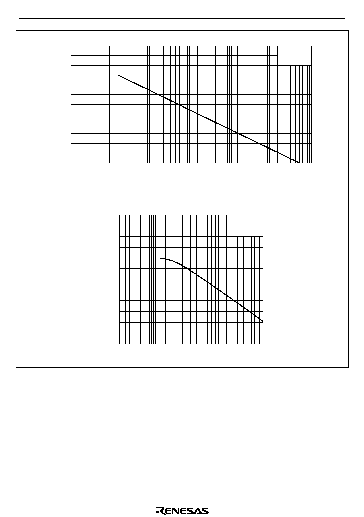
Voltage Gain vs. Frequency
V
CC
= 15V
Ta = 25
∞C
R
L
=
Voltage gain A
VD
(dB)
120
100
80
60
40
20
0
1
3
10
30
100
300
1 k
3 k
10 k
30 k
100 k 300 k
1 M
Frequency f (Hz)
V
CC
= 15V
Ta = 25
∞C
R
S
= 50
120
100
80
60
40
20
0
100
300
1 k
3 k
10 k
30 k
100 k 300 k
1M
Frequency f (Hz)
Common Mode Rejection Ratio vs. Frequency
Common mode rejection ratio CMR (dB)

HA17904A Series
Rev.0, May 2001, page 7 of 9
Solder Mounting Method
1. Small and light surface-mount packages require spicial attentions on solder mounting.
On solder mounting, pre-heating before soldering is needed.
The following figure show an example of infrared rays refow.
2. The difference of thermal expansion coefficeient between mounted substrates and IC leads may cause a
failure like solder peeling or soler wet, and electrical characteristics may change by thermal stress.
Therefore, mounting should be done after sufficient confirmation for especially in case of ceramic
substrates.
Temperature
140 to 160
∞C
1 to 5
∞C/s
235
∞C Max
10 s Max
1 to 4
∞C/s
Time (s)
60 s
Figure 1 An Example of Infrared Rays Reflow Conditions
HA17904A Series
Rev.0, May 2001, page 8 of 9
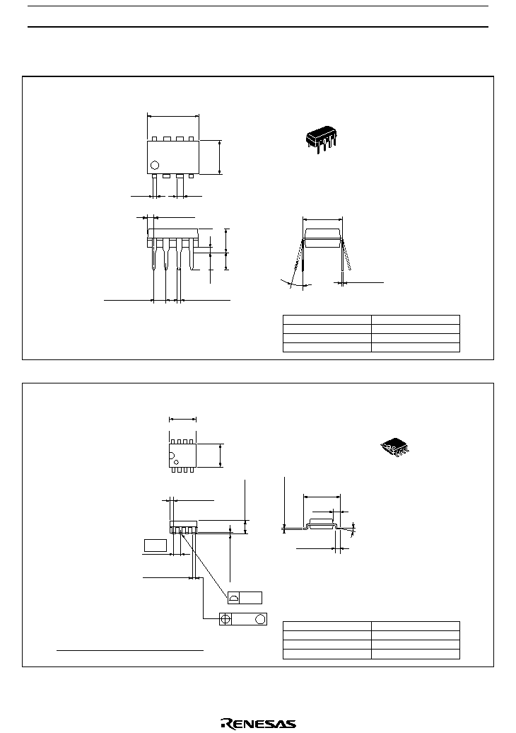
Package Dimensions
Hitachi Code
JEDEC
EIAJ
Mass (reference value)
DP-8B
Conforms
Conforms
0.51 g
Unit: mm
1
4
5
8
9.6
10.6 Max
0.89
1.3
6.3
7.4 Max
5.06 Max
2.54
± 0.25
0.48
± 0.10
7.62
0.25
+ 0.10
- 0.05
0
∞ - 15∞
2.54 Min
0.5 Min
1.27 Max
Hitachi Code
JEDEC
EIAJ
Mass (reference value)
FP-8D
--
Conforms
0.10 g
Unit: mm
*Dimension including the plating thickness
Base material dimension
0.10 ± 0.10
2.03 Max
4.4
*0.22 ± 0.05
4.85
0.75 Max
0.40 ± 0.06
0.60
+ 0.25
≠ 0.18
*0.42 ± 0.08
0.12
0.15
0∞ ≠ 8∞
M
8
5
1
4
1.05
5.25 Max
1.27
0.20 ± 0.04
6.50
+ 0.25
≠ 0.15

HA17904A Series
Rev.0, May 2001, page 9 of 9
Disclaimer
1. Hitachi neither warrants nor grants licenses of any rights of Hitachi's or any third party's patent,
copyright, trademark, or other intellectual property rights for information contained in this document.
Hitachi bears no responsibility for problems that may arise with third party's rights, including
intellectual property rights, in connection with use of the information contained in this document.
2. Products and product specifications may be subject to change without notice. Confirm that you have
received the latest product standards or specifications before final design, purchase or use.
3. Hitachi makes every attempt to ensure that its products are of high quality and reliability. However,
contact Hitachi's sales office before using the product in an application that demands especially high
quality and reliability or where its failure or malfunction may directly threaten human life or cause risk
of bodily injury, such as aerospace, aeronautics, nuclear power, combustion control, transportation,
traffic, safety equipment or medical equipment for life support.
4. Design your application so that the product is used within the ranges guaranteed by Hitachi particularly
for maximum rating, operating supply voltage range, heat radiation characteristics, installation
conditions and other characteristics. Hitachi bears no responsibility for failure or damage when used
beyond the guaranteed ranges. Even within the guaranteed ranges, consider normally foreseeable
failure rates or failure modes in semiconductor devices and employ systemic measures such as fail-
safes, so that the equipment incorporating Hitachi product does not cause bodily injury, fire or other
consequential damage due to operation of the Hitachi product.
5. This product is not designed to be radiation resistant.
6. No one is permitted to reproduce or duplicate, in any form, the whole or part of this document without
written approval from Hitachi.
7. Contact Hitachi's sales office for any questions regarding this document or Hitachi semiconductor
products.
Sales Offices
Hitachi, Ltd.
Semiconductor & Integrated Circuits
Nippon Bldg., 2-6-2, Ohte-machi, Chiyoda-ku, Tokyo 100-0004, Japan
Tel: (03) 3270-2111 Fax: (03) 3270-5109
Copyright © Hitachi, Ltd., 2001. All rights reserved. Printed in Japan.
Hitachi Asia Ltd.
Hitachi Tower
16 Collyer Quay #20-00
Singapore 049318
Tel : <65>-538-6533/538-8577
Fax : <65>-538-6933/538-3877
URL : http://www.hitachi.com.sg
URL
NorthAmerica
: http://semiconductor.hitachi.com/
Europe
: http://www.hitachi-eu.com/hel/ecg
Asia
: http://sicapac.hitachi-asia.com
Japan
: http://www.hitachi.co.jp/Sicd/indx.htm
Hitachi Asia Ltd.
(Taipei Branch Office)
4/F, No. 167, Tun Hwa North Road
Hung-Kuo Building
Taipei (105), Taiwan
Tel : <886>-(2)-2718-3666
Fax : <886>-(2)-2718-8180
Telex : 23222 HAS-TP
URL : http://www.hitachi.com.tw
Hitachi Asia (Hong Kong) Ltd.
Group III (Electronic Components)
7/F., North Tower
World Finance Centre,
Harbour City, Canton Road
Tsim Sha Tsui, Kowloon
Hong Kong
Tel : <852>-(2)-735-9218
Fax : <852>-(2)-730-0281
URL : http://semiconductor.hitachi.com.hk
Hitachi Europe GmbH
Electronic Components Group
Dornacher Straþe 3
D-85622 Feldkirchen, Munich
Germany
Tel: <49> (89) 9 9180-0
Fax: <49> (89) 9 29 30 00
Hitachi Europe Ltd.
Electronic Components Group
Whitebrook Park
Lower Cookham Road
Maidenhead
Berkshire SL6 8YA, United Kingdom
Tel: <44> (1628) 585000
Fax: <44> (1628) 585200
Hitachi Semiconductor
(America) Inc.
179 East Tasman Drive
San Jose,CA 95134
Tel: <1> (408) 433-1990
Fax: <1>(408) 433-0223
For further information write to:
Colophon 4.0