Regarding the change of names mentioned in the document, such as Hitachi
Electric and Hitachi XX, to Renesas Technology Corp.
The semiconductor operations of Mitsubishi Electric and Hitachi were transferred to Renesas
Technology Corporation on April 1st 2003. These operations include microcomputer, logic, analog
and discrete devices, and memory chips other than DRAMs (flash memory, SRAMs etc.)
Accordingly, although Hitachi, Hitachi, Ltd., Hitachi Semiconductors, and other Hitachi brand
names are mentioned in the document, these names have in fact all been changed to Renesas
Technology Corp. Thank you for your understanding. Except for our corporate trademark, logo and
corporate statement, no changes whatsoever have been made to the contents of the document, and
these changes do not constitute any alteration to the contents of the document itself.
Renesas Technology Home Page: http://www.renesas.com
Renesas Technology Corp.
Customer Support Dept.
April 1, 2003
To all our customers

Cautions
Keep safety first in your circuit designs!
1. Renesas Technology Corporation puts the maximum effort into making semiconductor products better
and more reliable, but there is always the possibility that trouble may occur with them. Trouble with
semiconductors may lead to personal injury, fire or property damage.
Remember to give due consideration to safety when making your circuit designs, with appropriate
measures such as (i) placement of substitutive, auxiliary circuits, (ii) use of nonflammable material or
(iii) prevention against any malfunction or mishap.
Notes regarding these materials
1. These materials are intended as a reference to assist our customers in the selection of the Renesas
Technology Corporation product best suited to the customer's application; they do not convey any
license under any intellectual property rights, or any other rights, belonging to Renesas Technology
Corporation or a third party.
2. Renesas Technology Corporation assumes no responsibility for any damage, or infringement of any
third-party's rights, originating in the use of any product data, diagrams, charts, programs, algorithms, or
circuit application examples contained in these materials.
3. All information contained in these materials, including product data, diagrams, charts, programs and
algorithms represents information on products at the time of publication of these materials, and are
subject to change by Renesas Technology Corporation without notice due to product improvements or
other reasons. It is therefore recommended that customers contact Renesas Technology Corporation
or an authorized Renesas Technology Corporation product distributor for the latest product information
before purchasing a product listed herein.
The information described here may contain technical inaccuracies or typographical errors.
Renesas Technology Corporation assumes no responsibility for any damage, liability, or other loss
rising from these inaccuracies or errors.
Please also pay attention to information published by Renesas Technology Corporation by various
means, including the Renesas Technology Corporation Semiconductor home page
(http://www.renesas.com).
4. When using any or all of the information contained in these materials, including product data, diagrams,
charts, programs, and algorithms, please be sure to evaluate all information as a total system before
making a final decision on the applicability of the information and products. Renesas Technology
Corporation assumes no responsibility for any damage, liability or other loss resulting from the
information contained herein.
5. Renesas Technology Corporation semiconductors are not designed or manufactured for use in a device
or system that is used under circumstances in which human life is potentially at stake. Please contact
Renesas Technology Corporation or an authorized Renesas Technology Corporation product distributor
when considering the use of a product contained herein for any specific purposes, such as apparatus or
systems for transportation, vehicular, medical, aerospace, nuclear, or undersea repeater use.
6. The prior written approval of Renesas Technology Corporation is necessary to reprint or reproduce in
whole or in part these materials.
7. If these products or technologies are subject to the Japanese export control restrictions, they must be
exported under a license from the Japanese government and cannot be imported into a country other
than the approved destination.
Any diversion or reexport contrary to the export control laws and regulations of Japan and/or the
country of destination is prohibited.
8. Please contact Renesas Technology Corporation for further details on these materials or the products
contained therein.

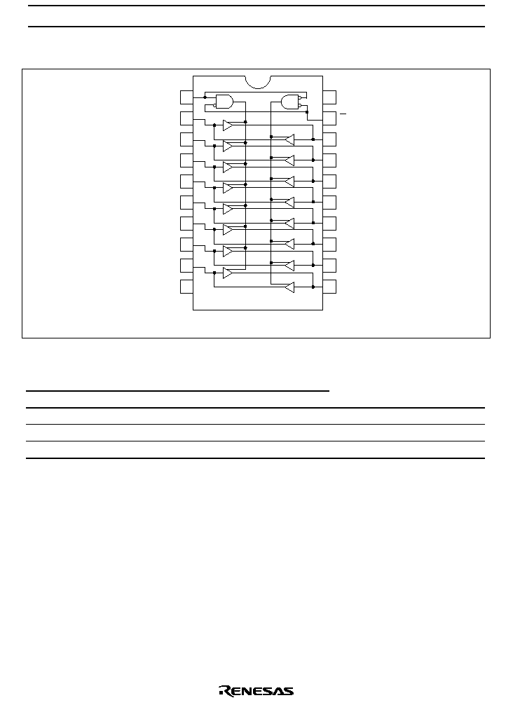
HD151245
Octal Bus Transceivers With 3 State Outputs
ADE-205-597 (Z)
1st. Edition
Dec. 2000
Description
The HD151245 featurs high speed operation and high drivability equivalent to the HD74LS245, which
realize ultra low power dissipation. This device consists of eight bus transceivers with three state outputs
in a 20 pin package. The device transmit data from the A bus to the B bus when the direction control (DIR)
input is at the high level,and from the B bus to the A bus when the DIR input is at the low level, the enable
input (
G) can be used to disable the device so that the buses are effectively isolated. The power up/down
protection provides the outputs in high impedance state when Vcc is low regardless of enable input.
Features
∑
High speed:
tpd = 10 ns typ.
∑
High output current:
I
OH
= ≠15 mA
I
OL
= 24 mA
∑
TTL Compatible Input/Output
∑
Wide operating temperature range: Ta = ≠40 to +85
∞
C
∑
High impedance state for both
Input/Output in power off condition.
∑
Power Up/Down Protection

HD151245
3
Absolute Maximum Ratings (Ta = 25
∞
C)
Item
Symbol
Rating
Unit
Supply Voltage
V
CC
≠0.5 to +7.0
V
Input Voltage(
G
, DiR)
V
IN
≠0.5 to +7.0
V
Input Voltage(A, B)
V
IN
≠0.5 to +5.5
V
Output Voltage
V
OUT
≠0.5 to +5.5
V
Power Dissipation
P
T
500
mW
Storage Temperature Range
Tstg
≠65 to +150
∞
C
Note:
1. The absolute maximum ratings are values which must not individually be exceeded, and
furthermore, no two of which may be realized at the same time.
Recommended Operating Conditions
Item
Symbol
Min
Typ
Max
Unit
Supply Voltage
V
CC
4.5
5.0
5.5
V
Output Current
I
OH
--
--
≠15
mA
I
OL
--
--
24
mA
Operating Temperature
Topr
≠40
25
85
∞
C
Input Rise and Fall Time*
1
t
r
, t
f
0
--
250
ns/V
Note:
1. This item guarantees maximum limit when one input switches.
Waveform: Refer to test circuit of switching characteristics.