Rev.2.00, May.12.2003, page 1 of 30
HD151TS201SS/T
Mother Board Clock Generator
for Intel P4 Chipset
REJ03D0007≠0200Z
Preliminary
Rev.2.00
May.12 2003
Description
The HD151TS201 is Intel CK408 type high-performance, low-skew, low-jitter, PC motherboard Clock
generator. It is specifically designed for Intel PentiumÆ4 chipset.
Features
∑
3 differential pairs of current mode control CPU clock
∑
7 PCI clocks and 3 PCIF clocks @3.3V, 33.3MHz typ.
∑
1 copy of 48MHz for USB @3.3V
∑
1 copy of 48MHz for DOT @3.3V
∑
6 copies of 3V66 clock @3.3V,66.6MHz
∑
1 copy of VCH@3.3V, 48MHz
∑
Power save and clock stop function.
∑
I
2
C
TM
serial port programming
∑
Programmable Clock Control (Spread Spectrum Percentage, Clock Output Skew, Slew Rate)
∑
56pin SSOP (300 mils) :
HD151TS201SS
∑
56pin TSSOP (244 mils) :
HD151TS201T
∑
Ordering Information
Part Name
Package Type
Package Code
Package
Abbreviation
Taping
Abbreviation (Quantity)
HD151TS201SSEL
SSOP-56 pin
SS
HD151TS201TEL
TSSOP-56 pin
T
EL (1,000 pcs / Reel)
Note: Please consult the sales office for the above package availability.
Note:
I
2
C is a trademark of Philips Corporation.
Pentium is registered trademark of Intel Corporation

HD151TS201SS/T
Rev.2.00, May.12.2003, page 2 of 30
Key Specifications
∑
Supply Voltages: VDD = 3.3V±5%
∑
CPU Clock cycle to cycle jitter = |150ps|
∑
CPU clock group Skew = 100ps
∑
3V66 clock group Skew = 250psmax
∑
PCI clock group Skew = 500psmax
HD151TS201SS/T
Rev.2.00, May.12.2003, page 3 of 30
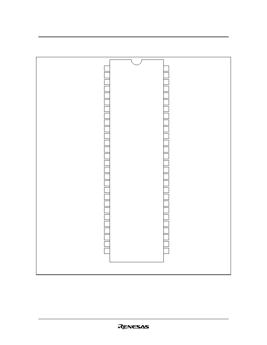
Pin Arrangement
1
2
3
4
5
6
7
8
9
10
VDD
XIN
XOUT
GND
PCIF0
PCIF1
PCIF2
VDD
PCI0
PCI1
PCI2
PCI3
VDD
GND
PCI4
PCI5
PCI6
VDD
GND
66OUT0/3V66_2
66OUT1/3V66_3
66OUT2/3V66_4
66IN/3V66_5
GND
11
12
13
14
15
16
17
18
19
20
21
22
23
24
33
34
35
36
37
38
39
40
41
42
43
44
45
46
47
48
49
50
51
52
53
54
55
56
3V66_0
PCISTOP#
3V66_1/VCH
VDD48
DOT48
CPUCLKC2
S2
GND IREG
CPUCLKT2
GND
CPUCLKC1
CPUCLKT1
USB48
VDD
CPUCLKC0
CPUCLKT0
S0
REF
S1
GND48
PWRDWN#
VDDA
GNDA
VTT_PWRGD#
25
26
27
28
29
30
31
32
SDATA
SCLK
GND
VDD
IREF
MULT0
VDD
CPUSTOP#
(Top view)
PCISTOP#, MULT0, PWRDWN#, CPUSTOP# = 150K
Internal Pull-up
HD151TS201SS/T
Rev.2.00, May.12.2003, page 4 of 30
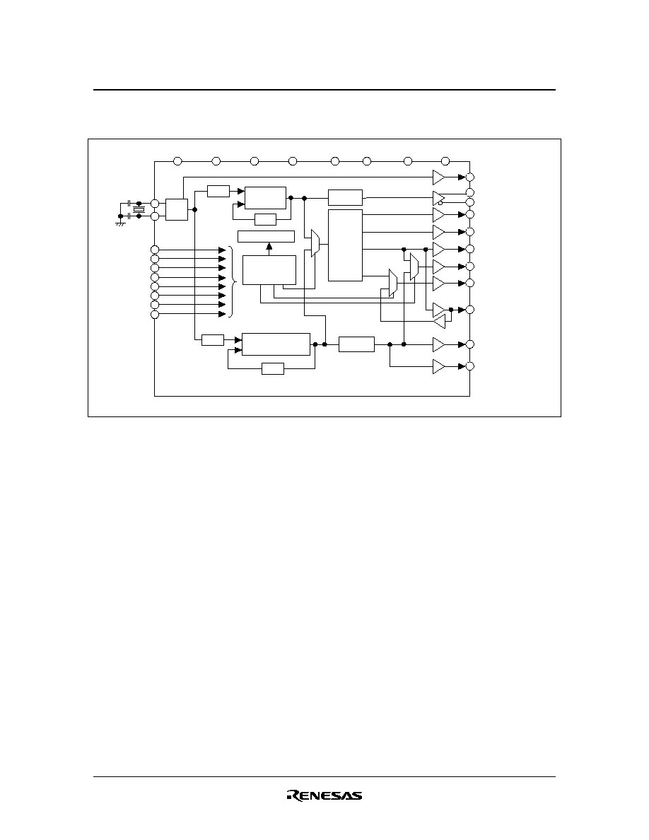
Block Diagram
CPU PLL
Control
Logic
1/n1
OSC
XTAL
14.318 MHz
SSC Modulator
REF(14.318 MHz)
CPUCLK(0:2)
PCI(0:6)
Note: Latched Input / Multi Function pin.
3.3 V VDD48
GNDA
GND48 3.3V VDDA
7
◊
3.3V VDD 6
◊
GND
GNDIREF
IREF
3V66_1/VCH
3V66_0
PCIF(0:2)
USB48
*S0, 1, 2
SCLK
SDATA
CPUSTOP#
*MULT0
PWRDWN#
PCISTOP#
VTT_PWRGD#
1/n2
1/m2
1/m1
Divider
Divide
3V66(2:4)/66OUT(0:2)
(66MHz)
66IN/3V66_5
(IN/OUT)
DOT48
Divider
48 MHz USB PLL

HD151TS201SS/T
Rev.2.00, May.12.2003, page 5 of 30
Table1 Clock Frequency Function Table & I
2
C
Byte8 (bit1, 2, 3, 4, 5)
Bit5
Bit4
Bit3
Bit2
Bit1
CPU
3V66
PCI
0
0
0
0
0
0
66.67
66.67
33.33
1
0
0
0
0
1
70
70
35
2
0
0
0
1
0
75
66.67
33.33
3
0
0
0
1
1
80
66.67
33.33
4
0
0
1
0
0
85
66.11
33.06
5
0
0
1
0
1
90
67.5
33.75
6
0
0
1
1
0
95
66.5
33.25
7
0
0
1
1
1
100
66.67
33.33
8
0
1
0
0
0
105
70
35
9
0
1
0
0
1
110
66
33
10
0
1
0
1
0
115
65.71
32.86
11
0
1
0
1
1
120
66.67
33.33
12
0
1
1
0
0
125
69.44
34.72
13
0
1
1
0
1
130
65
32.5
14
0
1
1
1
0
133.33
66.67
33.33
15
0
1
1
1
1
135
67.5
33.75
16
1
0
0
0
0
140
70
35
17
1
0
0
0
1
145
64.44
32.22
18
1
0
0
1
0
150
50
25
19
1
0
0
1
1
150
66.67
33.33
20
1
0
1
0
0
155
66.43
33.21
21
1
0
1
0
1
160
68.57
34.29
22
1
0
1
1
0
165
66
33
23
1
0
1
1
1
166.67
55.56
27.78
24
1
1
0
0
0
166.67
66.67
33.33
25
1
1
0
0
1
170
68
34
26
1
1
0
1
0
175
70
35
27
1
1
0
1
1
180
67.5
33.75
28
1
1
1
0
0
185
69.38
34.69
29
1
1
1
0
1
190
63.33
31.67
30
1
1
1
1
0
195
65
32.5
31
1
1
1
1
1
200
66.67
33.33